1. INTRODUCTION Traditional fabrication technologies are originated for the process developed for silicon integrated circuit fabrication. So, there processes are usually designed for creating planar structures on the material like silicon. Therefore, vertical sidewalls are easily achieved through dry anisotropic etching process; however, fabricating angled sidewalls are quite hard to make it. Gray-scale lithography is a one of useful batch process to create gradient height structures for angled sidewalls. Below fig. 1 shows how to work gray-scale lithography.
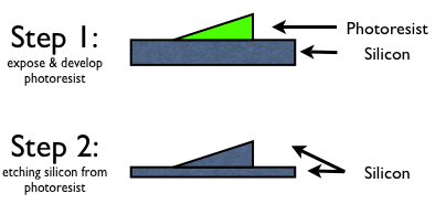
Fig. 1: Two Step Process to fabricate angled sidewalls
2. THEORY
(a) Basic Concept Why are gradient height structures on photoresist created in step 1 of fig. 1? The reason is that gray-scale lithography changes exposure dose locally to develop the 3D structure in the photoresist. So, differential exposure dose make differential depth of exposed photoresist across the surface. This is because the photoactive compound is absorbing the ultraviolet light energy as it travels in the depth of the photoresist. By using chrome-on-glass (COG) masks, which induces diffraction, the ultraviolet intensity can be modulated.
(b) Diffraction Now, we know gray-scale lithography is using diffraction to modulate intensity of the ultraviolet. Then, what is the diffraction? It is defined that diffraction is the bending, spreading and interference of waves when they pass by an obstruction or through a gap. (From Wikipedia) For example, if wave source is passing through single slit, which is narrower than wavelength of wave, bending & spreading of waves to pass around obstacle form semicircular ripple. This is the diffraction pattern, and it is approximately equally strong in all directions as if there is a simple wave source at the center of single slit.
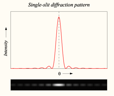
Fig. 2: Graph and image of single-slit diffraction (from Wikipedia)
(* There is useful applet to show light diffraction through periodic grating in the following link. LINK)
(c) Diffraction & Gray-scale Mask Lithography Diffraction occurs in projection lithography using a COG mask patterned with opaque pixels when both the size and the pitch of the pixels are close to or below the resolution of the given lithography system. (Fig. 3)
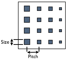
Fig. 3: Pitch & Size of the pixels
When diffraction occurs, light passing through mask breaks up into spatial diffraction orders. (0, +1, -1, +3, -3,) (See Fig. 2) This order tells that the amplitude of the intensity. The objective lens collects these diffraction orders according to its numerical aperture and will reconstruct the pixels on the photoresist surface if at least the 0 and one of the first (+1 or -1) diffraction orders are captured as shown in Fig. 4(a). However, when the pixels and pitch are small enough, only the 0 order is captured by the objective lens and focused onto the photoresist as shown Fig. 4(b). (* To know detail of numerical aperture, see the following site: LINK)
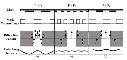
Fig. 4: Diffraction orders in the shaded region denote the orders not accepted by the numerical aperture of the objective lens in the lithography system
The intensity passing through the mask is dependent on the fill area of each pitch. For example, if the mask is designed with square pixels and a set pitch between pixels as is shown in Fig. 5, then the intensity depends on the percentage of the opaque area for each pitch area. In this case the pitch is chosen to be below the resolution of the projection system so that the distance between each pixel remains below resolution. So, the pixel size can be modified to modulate directly the intensity passing through the objective lens. Another method to change the intensity is to keep the size of the pixel constant and change only the pitch, or it is possible to change both the size and the pitch. Actually, first method, changing only pixel size is easy to design the mask.
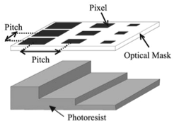
Fig. 5: Mask Example using constant pitch & variable pixel size
(d) Design Limitation of the Gray-scale Mask The number of gray levels is dependent on the resolution and magnification of the projection lithography system, along with the minimal pixel size and increment between subsequent pixel sizes. The number of gray levels determines the roughness or exact definition of the profile in the photoresist. There is a resolution limit on the minimum pixel size for a given projection lithography system, which sets the upper limit for the area and spacing on the mask. Therefore. Due to the diagonal spacing between two pixels being the largest spacing, an approximation of the minimum pixel size can be shown by the equation

(Wmin is the minimum pixel width, P is the pitch chosen for the mask and Pc is the resolution of the projection system) * For example, projection system resoluion is 3.5 μm. We set pitch to 3.5 μm. Then, minimum pixel width is about 1 μm.
If pixel has dimension below the minimum pixel width, it causes the photoresist to fully develop. Maximum pixel size is up to the pitch size. According to these values, we can set possible maximum the number of gray levels. The pitch can be changed to vary the size of the structure. However, just above the resolution of the projection lithography, oscillations in the aerial image intensity will occur. (See Fig. 4(c)) The heights of the gray levels depend on many factors, primarily the initial photoresist thickness, the aerial image intensity for each gray level, the absorption coefficient which gives the concentration of both the photoactive compound remaining and exposure product produced, the time of development and the contrast of the photoresist. So, a calibration mask with multiple gray-scale patterns of different pitches and with all available pixels can be used to find both design limits & thickness.
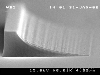
Fig. 6: Gray-scale Mask Example developed AZ4620 photoresist with 3.5 μm pitch and one row per pixel size & 30 gray levels, thickness 5 μm, 25 μm long. Minimum pixel size is 0.4 μm with a 0.1 μm consecutive increment size between two pixel levels. As you see, below minimum pixel width, photoresist is developed fully. Minimum pixel width is about 1 μm.
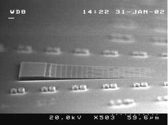
Fig. 7: Gray-scale Mask Example AZ4620 developed photoresist consisting of 22 height levels using a 3.5 μm pitch on the mask and ten rows per pixel size
- PhotoresistcharacterizationandlinearizationprocedureforGSM.pdf: Photoresist linearization procedure for GSM
- Microfabricationof3DsiliconMEMSstructuresusinggray-scalelithographyanddeepreactiveionetching.pdf: Fabrication of 3D silicon MEMS structure using GSM
Ideas, requests, problems regarding TWiki? Send feedback