new web: http://bdml.stanford.edu/pmwiki
TWiki > HSPrivate Web>HumanSafePrivate>OpticalForceSensors2d (27 Aug 2008, DanAukes)
2D Optical Force Sensors
Summary of Operation
The two-dimensional optical force sensor uses internally reflected light to sense forces applied to the surface of the skin. An optically clear flexible material is molded in a thin sheet, and rows of infrared-light-emitting emitters and sensors are embedded in the material in both the x and y directions. As forces are applied, light traveling through the material becomes obstructed from the phototransistors. By turning on one emitter at a time, an attached microcontroller can sense the analog voltage changes in each phototransistor. By building a pressure profile from each emitter/sensor combination, inferences can be made about the location, size, intensity, and number of contact forces acting on the sensor material.Benefits
There are several benefits of this design over other sensor array designs. First, by embedding emitters and sensors along the side of the rubber sheet, the need for intricate wire routing within the sensing area is eliminated. Sensor skins could be produced which cover a wide area, yet have minimal amounts of wiring. Second, because the optical medium is transparent rubber, the sensor is able to flex and conform to any surface. Third, because the one-dimensional arrays of sensors can be used to determine forces in two-dimensional space, there is a potential for reducing the number of individual transducers needed over other sensor designs. Finally, due to sensor placement and electrical design, the location and number of contact forces are not confounded, allowing for true multi-touch sensing within a single sheet.Manufacturing Summary
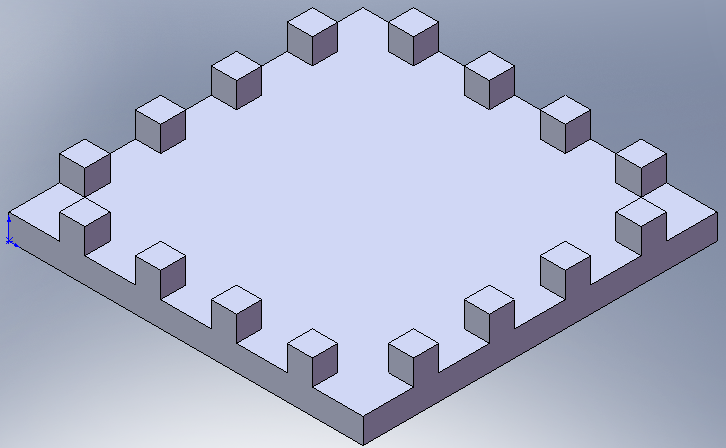
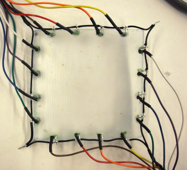 The optically-clear rubber part was designed in SolidWorks? , and then the negative of the part was milled in machining wax using a Haas CNC milling machine. Extra pockets were machined for placement of the electrical components, which were embedded in molding clay. ClearFlex50? polyurethane rubber was then poured over the mold, and the entire block was then vacuum-degassed. After curing, the electrical contacts were soldered to cables, shielded, and the entire device was connected to the rest of the circuitry.
2DSkinSensor.SLDPRT: Solidworks File of the Skin Sensor Positive Part
The optically-clear rubber part was designed in SolidWorks? , and then the negative of the part was milled in machining wax using a Haas CNC milling machine. Extra pockets were machined for placement of the electrical components, which were embedded in molding clay. ClearFlex50? polyurethane rubber was then poured over the mold, and the entire block was then vacuum-degassed. After curing, the electrical contacts were soldered to cables, shielded, and the entire device was connected to the rest of the circuitry.
2DSkinSensor.SLDPRT: Solidworks File of the Skin Sensor Positive Part
Material Selection
The skin is made from transparent polyurethane rubber called ClearFlex? 50, which is available from a company named Smoothon. Currently we are investigating several types of rubber, each with inherent tradeoffs.- ClearFlex? 50 ClearFlex? 50 is quite transparent, with an index of refraction around 1.5. It does not tear or break easily, but is also quite stiff, and has some mechanical hysteresis. Since it is a polyurethane rubber, it should be able to bond to many other materials, including other polyurethane rubbers. It may also be able to be painted
- Rubber Glass II Rubber Glass II is a silicone-based rubber, which gives it quite different properties from ClearFlex? . It seems to be more transparent than ClearFlex? , and is a much softer material. It seems to also have less mechanical hysteresis when deformed, as it springs back to shape much faster. Because it is a silicone-based material, however, it cannot be coated or painted, and should only adhere/cure with other silicone rubbers (although we have not investigated which/how many others it will adhere to). It is also extremely brittle, making it more difficult to work with.
- VytaFlex? 10-60 Several other polyurethane rubbers may work, despite the fact they are not completely transparent. Smoothons VytaFlex? line has somewhat better mechanical properties than ClearFlex? . These materials may obscure more light than other rubbers, limiting the eventual size of final patches, but this may be a small tradeoff for the better mechanical properties.
Electrical Design
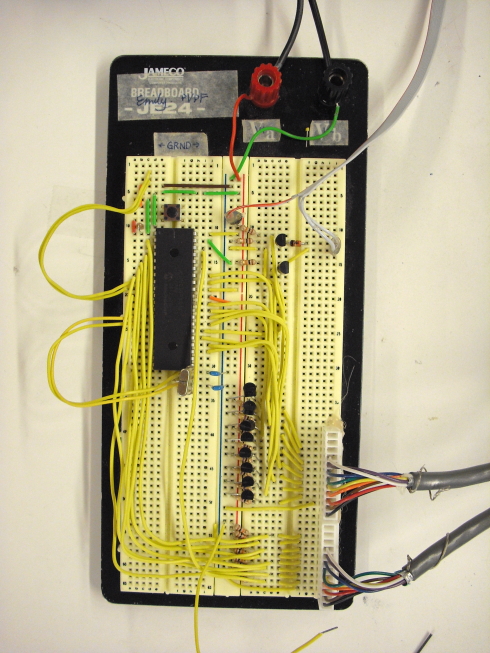
The electrical layout of the sensor is quite simple. Each infrared LED is turned on with a small-signal MOSFET controlled directly by a PIC microcontroller, and the current going through it is regulated by a 47 Ohm resistor sized to provide the maximum allowable .1 Amp of current. Each sensor is connected directly to an analog input line of the microcontroller, which reads the value of the sensor as each emitter is turned on. The rest of the circuitry on the microcontroller regulates the oscillator speed, processor reset, and serial communication to the attached computer. The PIC30f4013 microcontroller was selected because of its relatively high analog resolution (12-bit). It is programmed to turn on each emitter one by one, gather the analog voltages at each sensor, and compile those values into an 8x8 table, which it sends serially to the computer every 0.02s(50Hz). This speed is a limitation of the serial transmission alone, and can be greatly increased if another communication protocol is used in the future. 2DSkinSchematic.zip: Circuit Schematic Project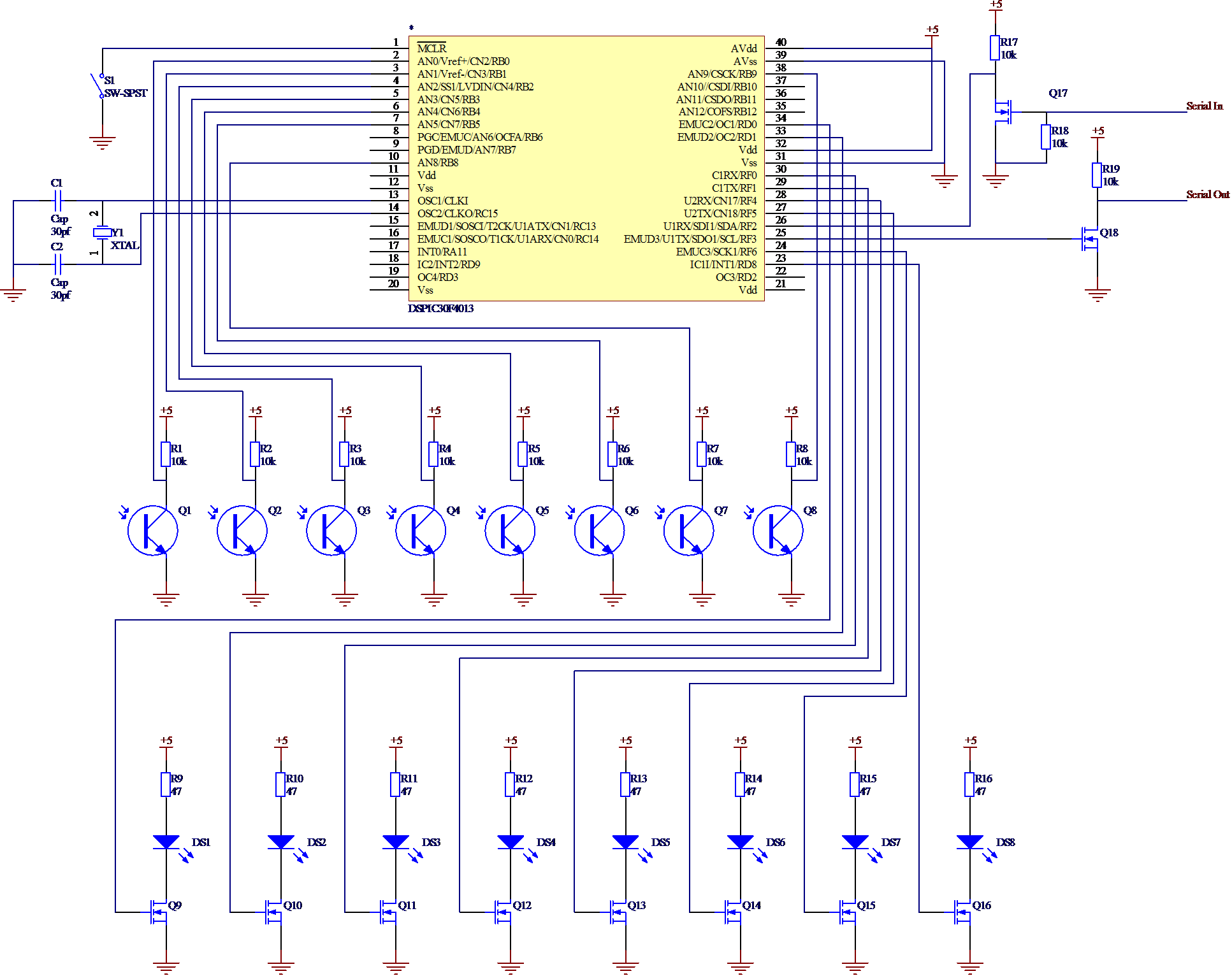
Computer Interface
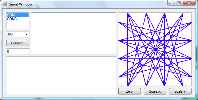
A simple computer program has been created to receive serial data from the microcontroller and provide visualization of the sensor data. The 8x8 data table sent by the microcontroller is parsed and represented as a series of rays pointing from each emitter to each sensor.- 2DSkinPIC.zip: PIC Program for controlling and sensing skin
- 2DSkinInterface.zip: Visual Studio Program for communicating and viewing PIC data
- Image of VisualStudio Interface:
Next steps
There are many areas open for continuing research with regard to this sensor. They include the following:- Characterize sensing modes The sensor is thought to employ the principle of frustrated total internal reflection. By further characterizing the method by which the sheet can sense pressure, we can make new designs that capitalize on that additional knowledge.
- Determine the type of surface effects which affect sensing, and determine ways to control them.
- Determine the types of deformation (compression, bending, etc) which most affect sensing.
- Measure the refraction indices of the materials involved, and extrapolate that data to other materials that may work better.
- Increase sensitivity and reduce noise - The mechanical stiffness of the rubber sheet inhibits small force measurements at the minimum specified force. Sensitivity can be increased in several ways:
- Optimize the geometry of the existing rubber sheet. By adding three-dimensional structures to the surface of the sheet, the sheet can be induced to bend or compress in ways other than simple compression when forces are applied, inducing larger signal swings at smaller forces.
- Pick better materials. The internal reflection inside the sheet is a result of the difference in optical transmission between the rubber sheet and the air. By changing the rubber, or by adding a new layer of rubber, coating, painting, etc, we could greatly increase sensitivity.
- Design new multi-material structures which can select for higher sensitivity where and how we want it, and can reduce the noise of the sensing modes and locations we dont care about.
- Shrink components create a new electrical design which captures the essence of the first design but which can be fully embedded into the final skin design by using flexible and/or conformable materials.
- Create localization and intensity algorithms which accurately compute the location, size, intensity, and number of contacts on the surface of the skin.
- Move more computation to the microcontroller. The more computation we can move to the microcontroller, the less data will have to be transmitted and processed by the final master controller.
Ideas, requests, problems regarding TWiki? Send feedback