Frequency Mode Capacitive Sensor Array
Overview
Capacitors make natural strain or force sensing devices because capacitance is directly related to the geometric configuration of the conductors in a capacitor. In the classic parallel plate example, as plates move closer together capacitance increases. This effect can be exploited to make an effective force sensor with excellent noise immunity, high accuracy, high resolution, low power consumption, and fast sampling time.
Circuit Design
|
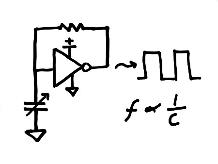
This extremely simple circuit uses a Schmitt inverter, a resistor, and a capacitor to create an oscillating output. The frequency of the output depends on many factors such as resistance, capacitance, hysteresis voltage, slew rate, etc. Luckily, many of these factors can be made relatively constant by design, so that a single isolated variable is used to affect the oscillation frequency. In our case, the capacitance is the only value that is allowed to change.
|
Basic multivibrator schematic:
|
|
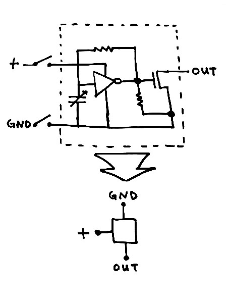
With a small modification to the output of the multivibrator circuit above, many outputs can be tied together without causing a short circuit. The open drain configuration shown here allows individual outputs to become active at a time, but won't cause damage if multiple outputs are activated simultaneously.
|
Open drain output on multivibrator circuit:
|
|
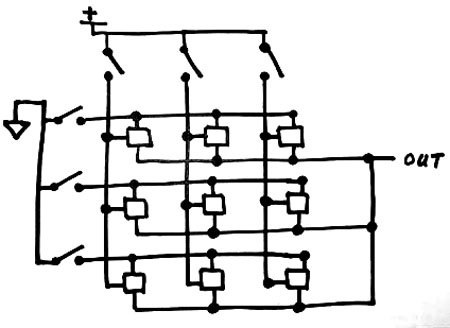
Due to the simplicity of the capacitance measurement circuit, it can be replicated many times to create a sensor array. Individual sensors are addressed by making the correct power and ground lines active. Otherwise, the power lines are held in a high impedance state. This is a simple task for a microcontroller, and requires a relatively small number of wires (and pins), especially in larger networks. One of the greatest features of this design is that there is only a single sensor output wire to send to the microcontroller. A simple pulse timer program is sufficient to make highly acccurate frequency measurements. Time multiplexing allows scanning of all sensors in the array.
|
Capacitive sensor array configuration:
|
|
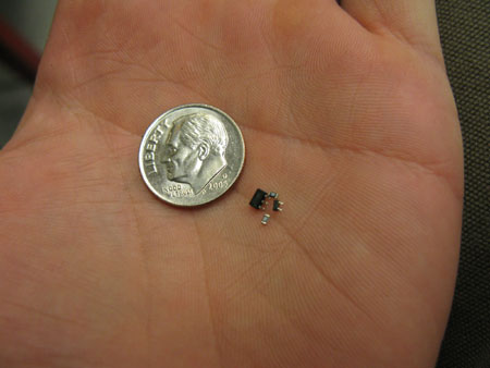
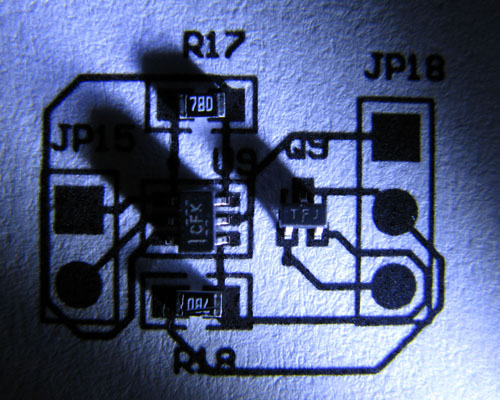
Only four inexpensive surface mount components are needed to make each capacitance measurement circuit. Thanks to surface mount technology, the form factors are quite small. The components shown aren't even the smallest available. These were chosen merely because they can be soldered by hand --a desireable property during the prototyping phase.
|
A dual Schmitt inverter, MOSFET, and two resistors:
|
|
An initial layout has been completed for testing the circuit in an array format. This circuit will be built on a hard PCB as a functional test. Assuming that all goes well, the circuit will probably be moved to a flexible substrate to allow for conformability in a skin application.
|
Initial wide spaced layout for testing:
|
|
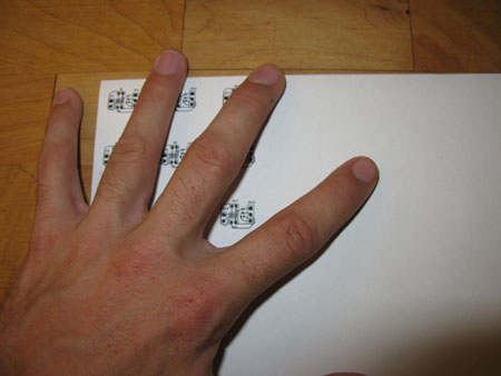
The initial PCB will consist of a 3x3 sensor array. All sensors are individually addressable with a single combined output wire.
|
3x3 sensor array layout with hand for scale:
|
Noise
Noise can be an issue with capacitive mode force sensing circuits. This is mainly due to two factors: improper shielding and long cable runs with analog signals. People often think that they can improve noise immunity by simply shielding the sensing wires that run to the measurement capacitance. Though this helps block external capacitive noise from coupling in, it also adds capacitance to the sensor because the shielded cable typically has a high capacitance itself. Essentially, this makes small changes in the sensing capacitor more difficult to detect because these changes are a smaller percentage of the overall capacitance being measured. Furthermore, a typical output mode for any sensor is an analog voltage. Though this makes a convenient, intuitive output, analog signals are susceptible to noise. This is especially true when long cable runs are necessary.
|
Noise control in the capacitive sensor array is accomplished with two-fold approach. The first part of the design implements a clever use of shielding. A shielding layer is certainly needed to make a force sensor immune to external noise, but the shielding layer should minimally affect the measurement of capacitance change with force application. In this design, the shielding layer is incorporated into the sensing capacitor and actually acts as one of the two plates in a parallel plate design. Not only does the circuit benefit from the shielding effect, it also has increased sensing capacitance because there are essentially parallel plate capacitors on each side of the center sensing plate!
|
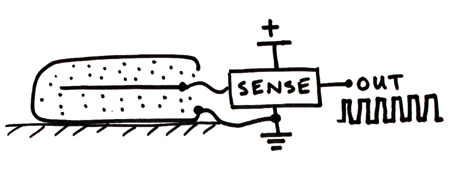
Shielded sensor design --the shield is part of the sensor!
|
|
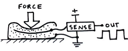
As the shielding layer is pressed, the capacitor deforms. The inner sensing plate and the outer shielding plates move closer increasing the capacitance. This decreases the frequency of the output. Note that the second main design feature is also highlighted here. Sensor noise is significantly reduced by using a digital pulse train output instead of an analog voltage. A pulse train can be sent over very long cables with poor shielding without signal degredation. The useful information, capacitance, lies in the frequency domain.
|
Force application deforms the sensor increasing its capacitance:
|
-- JohnUlmen - 06 Aug 2008
 HSPrivate Web>HumanSafePrivate>CapacitorArray (07 Aug 2008, DanAukes)