Week 10
August 22
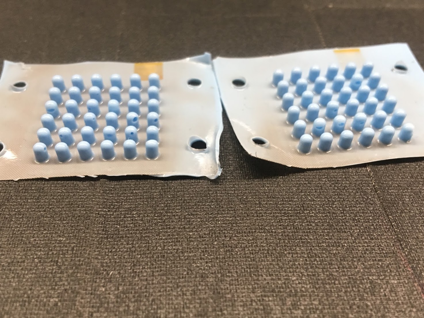
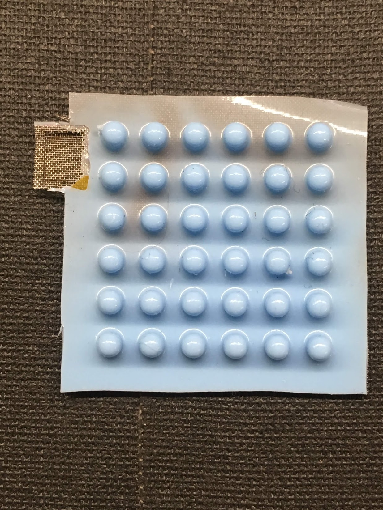
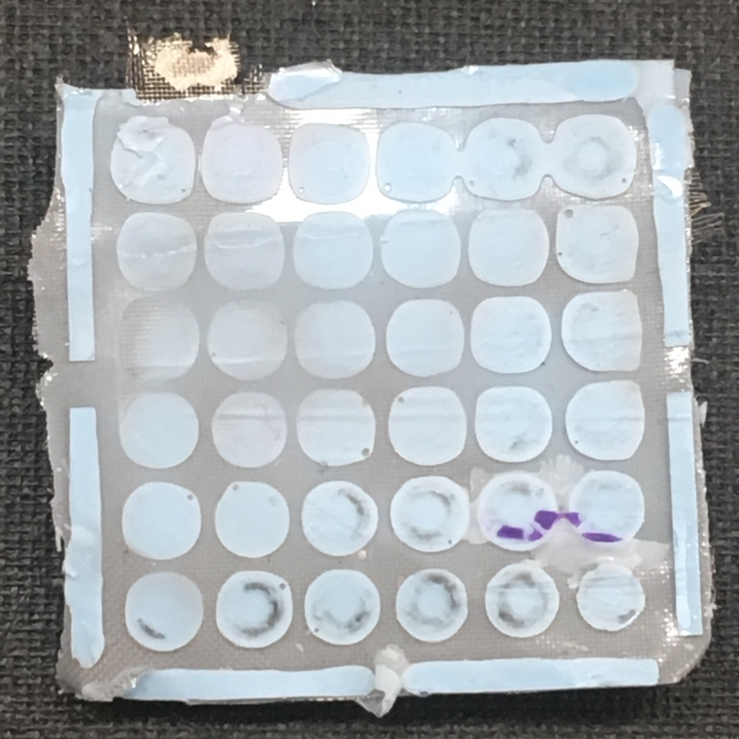
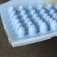
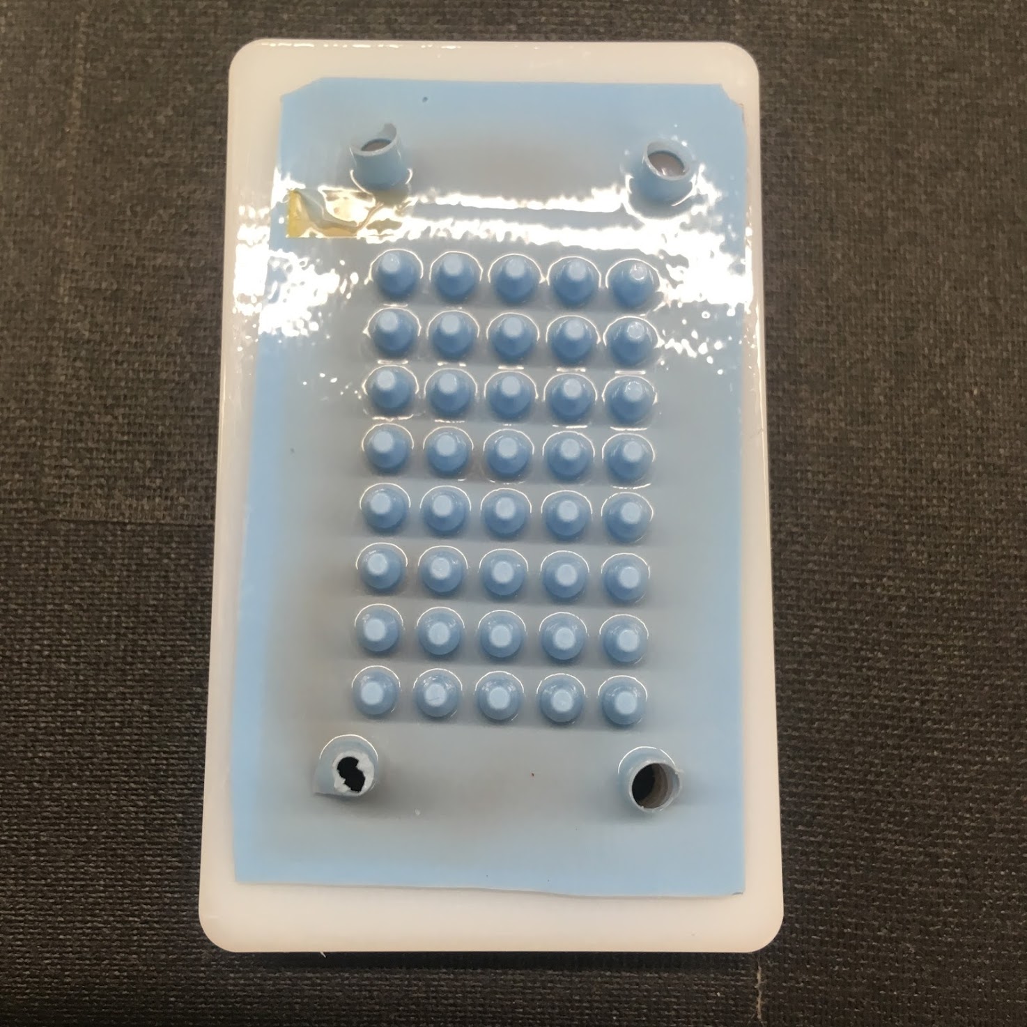
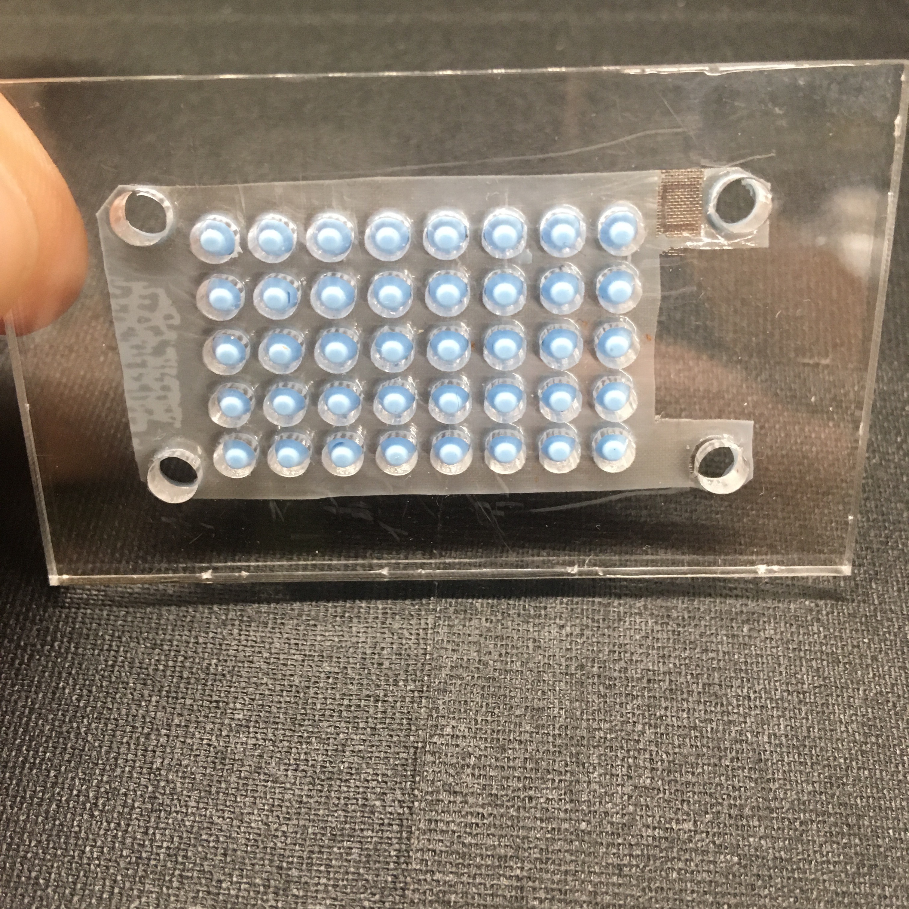
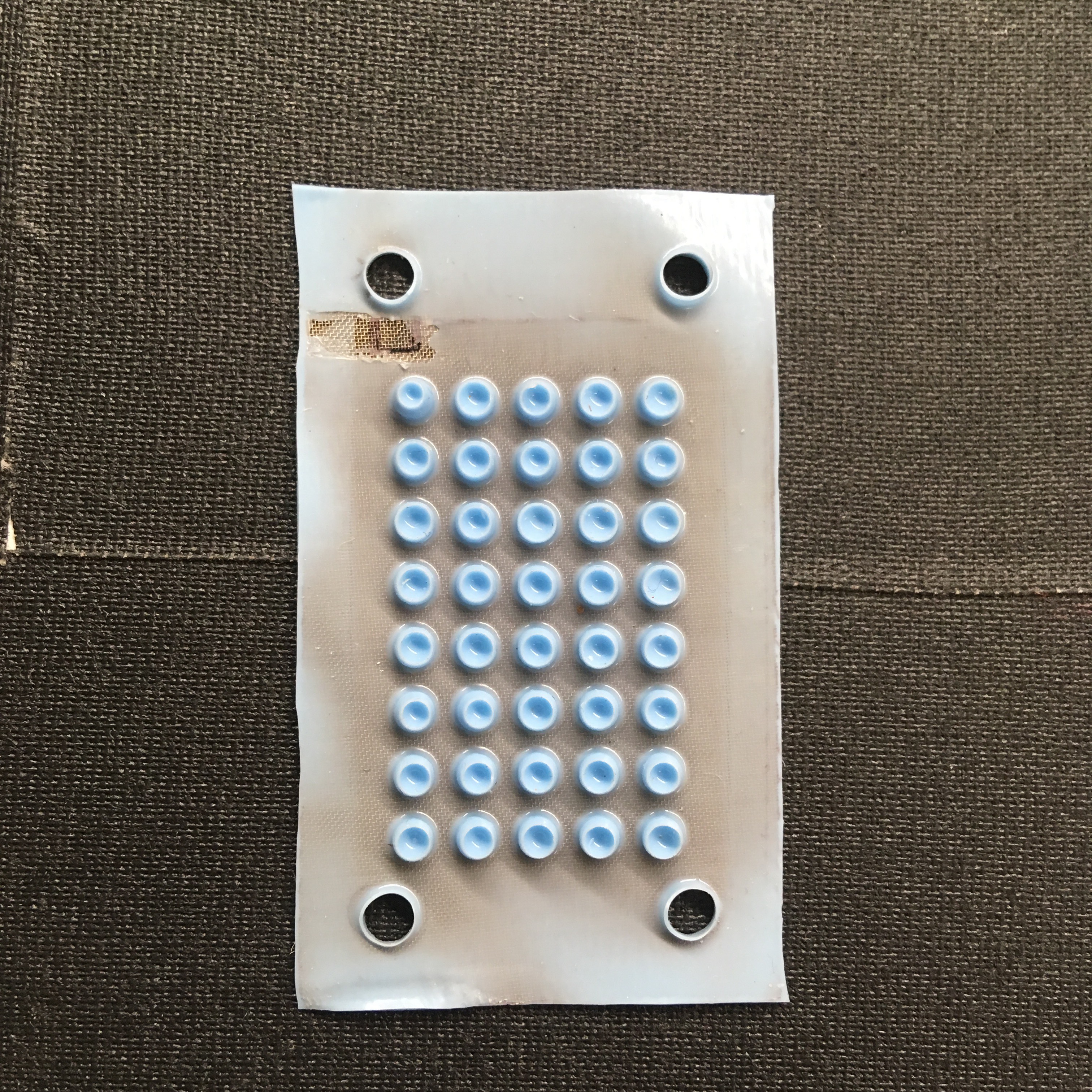
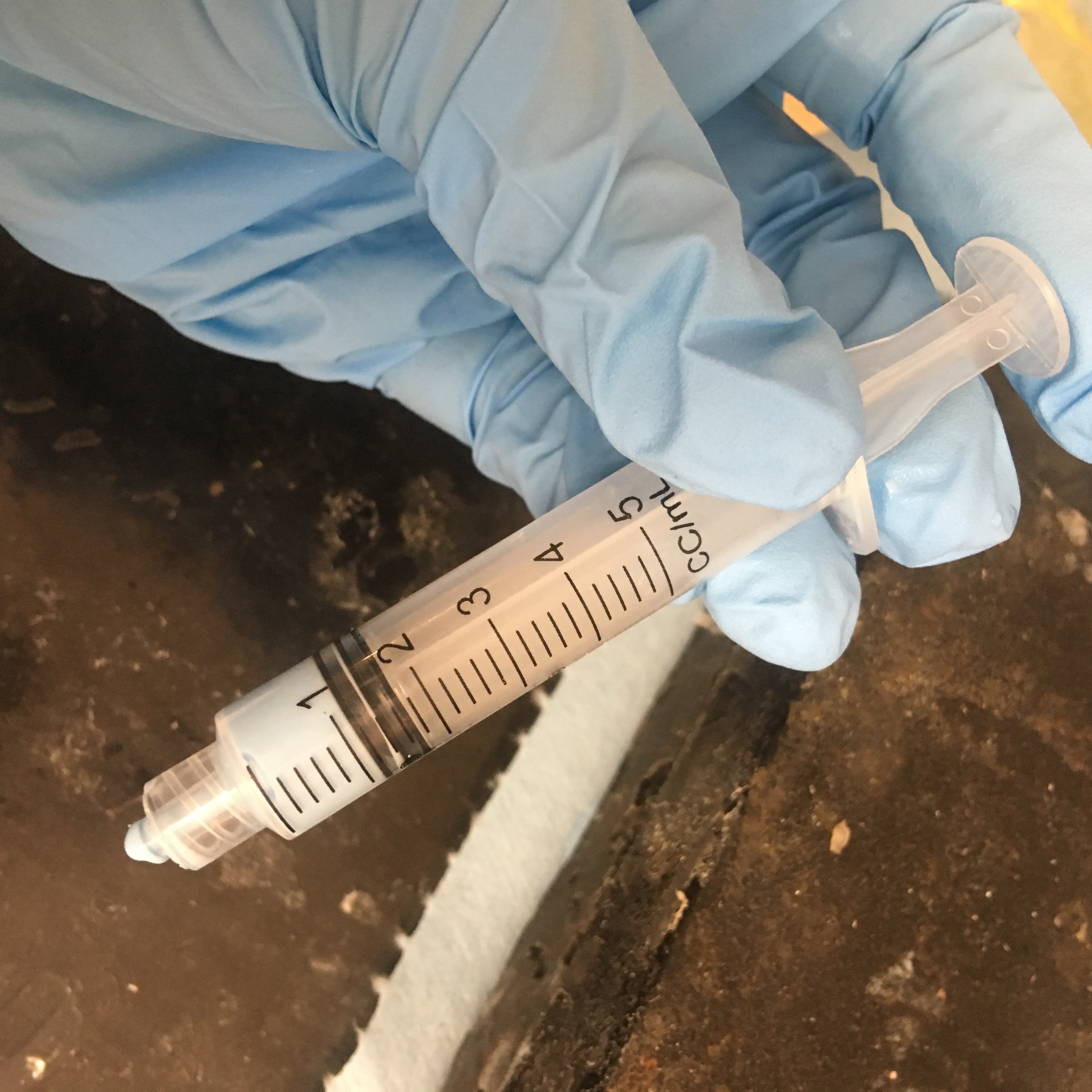
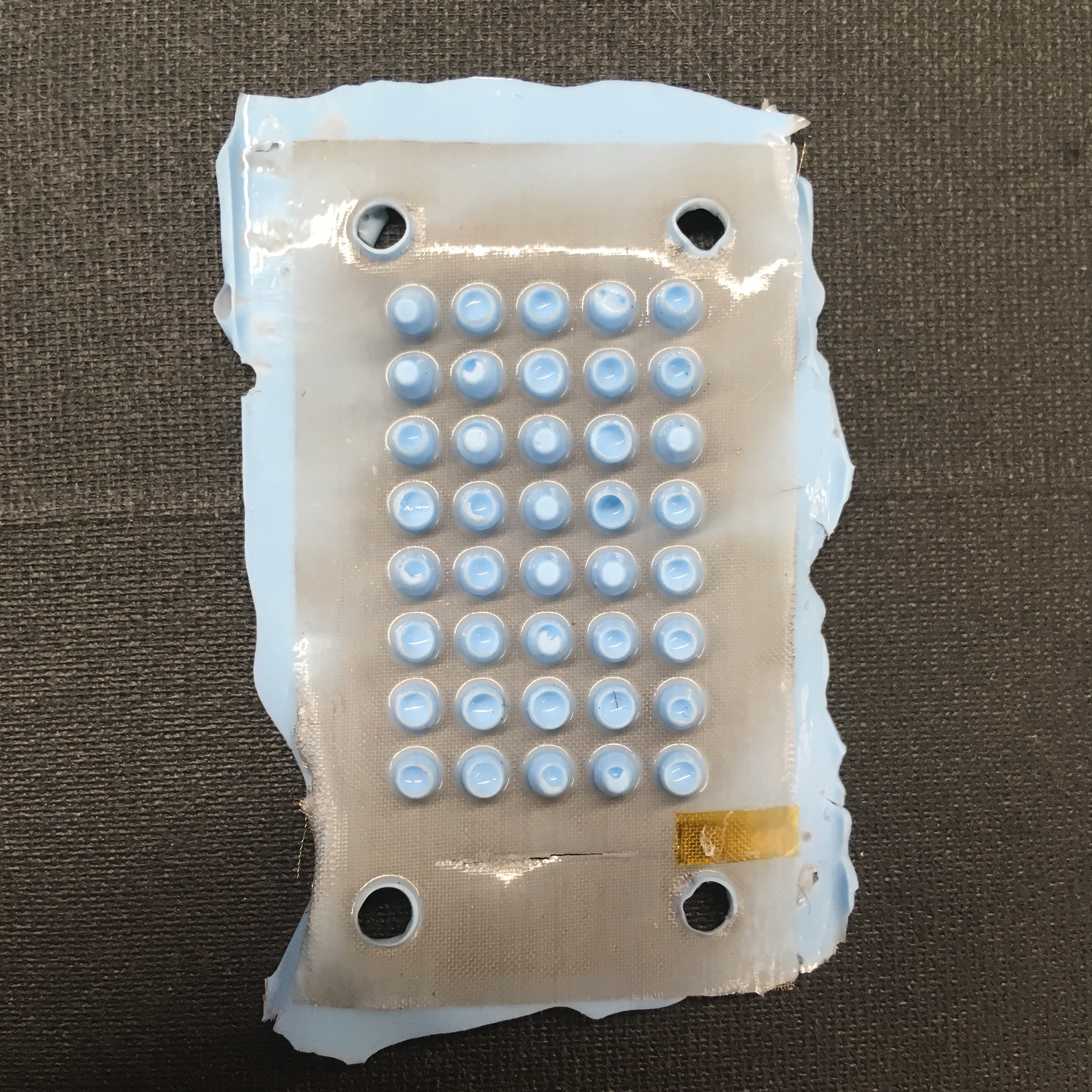
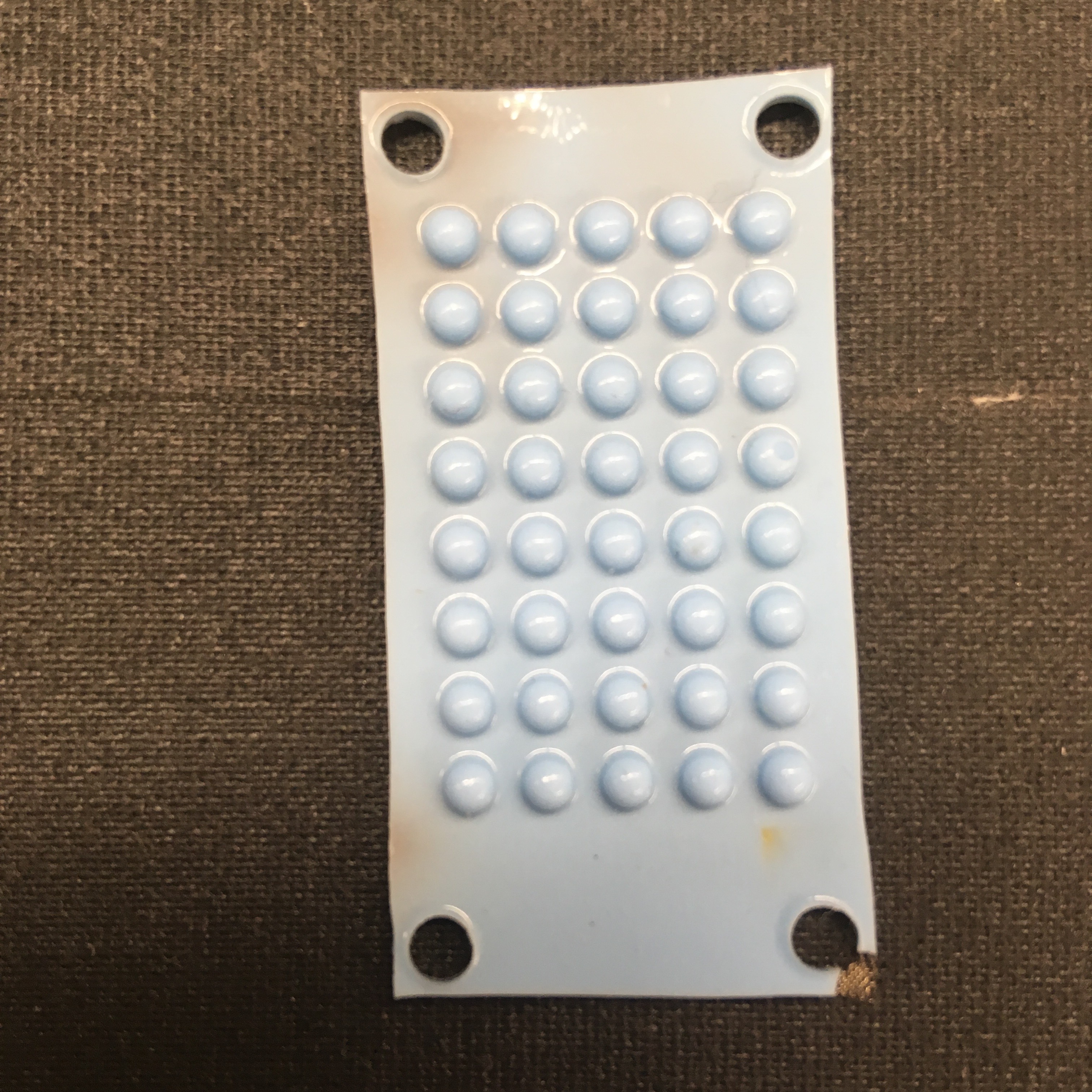
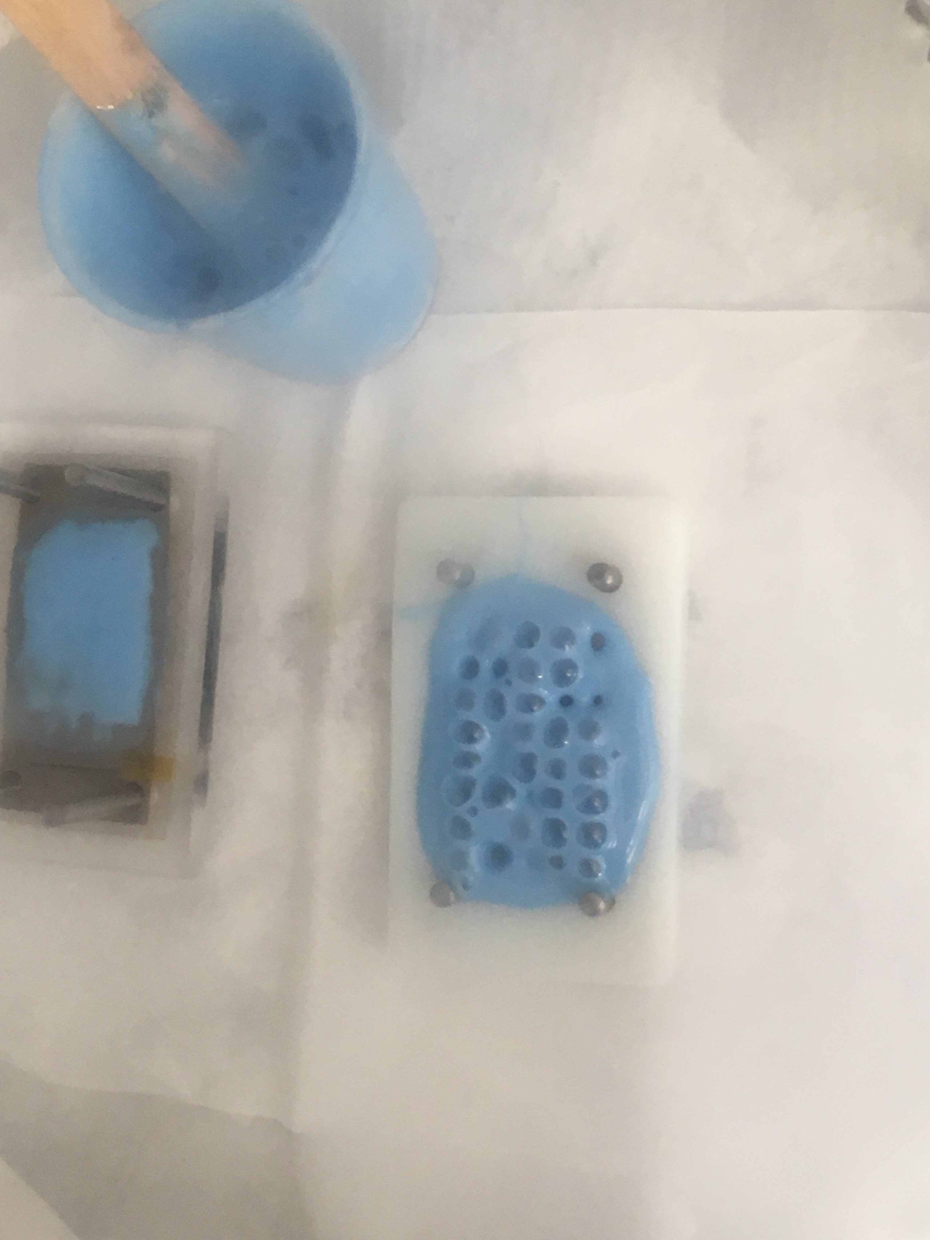
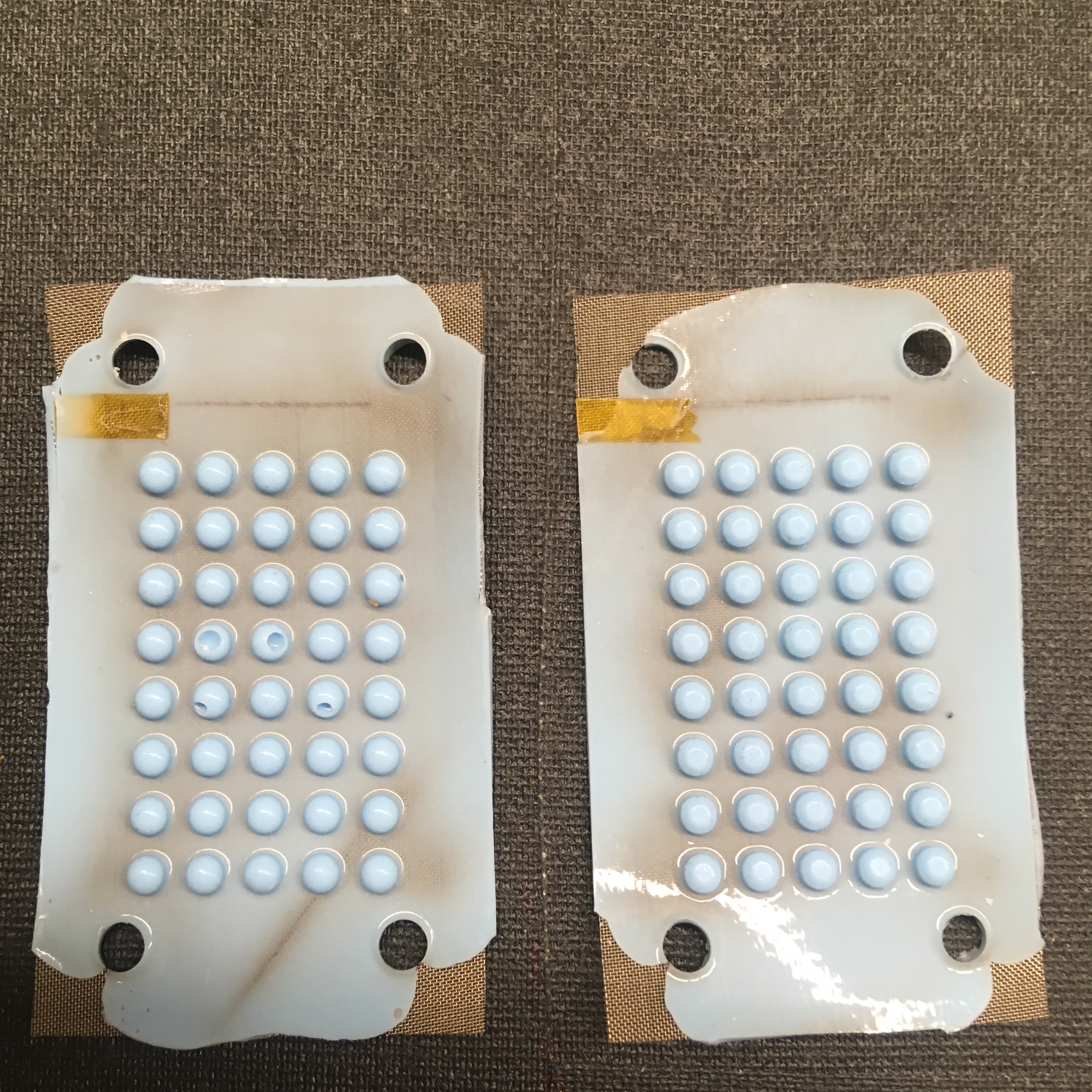
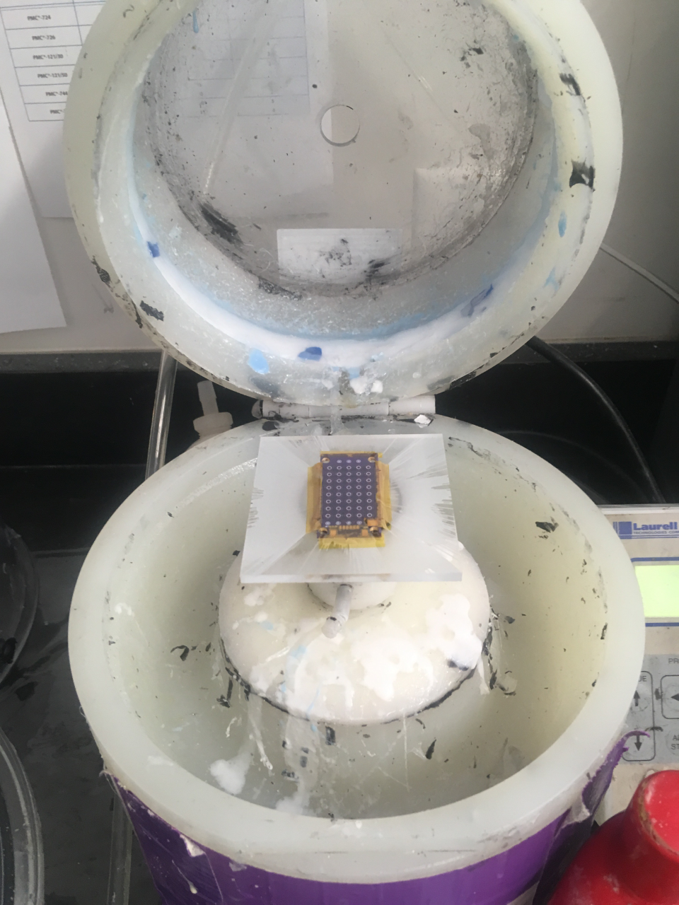
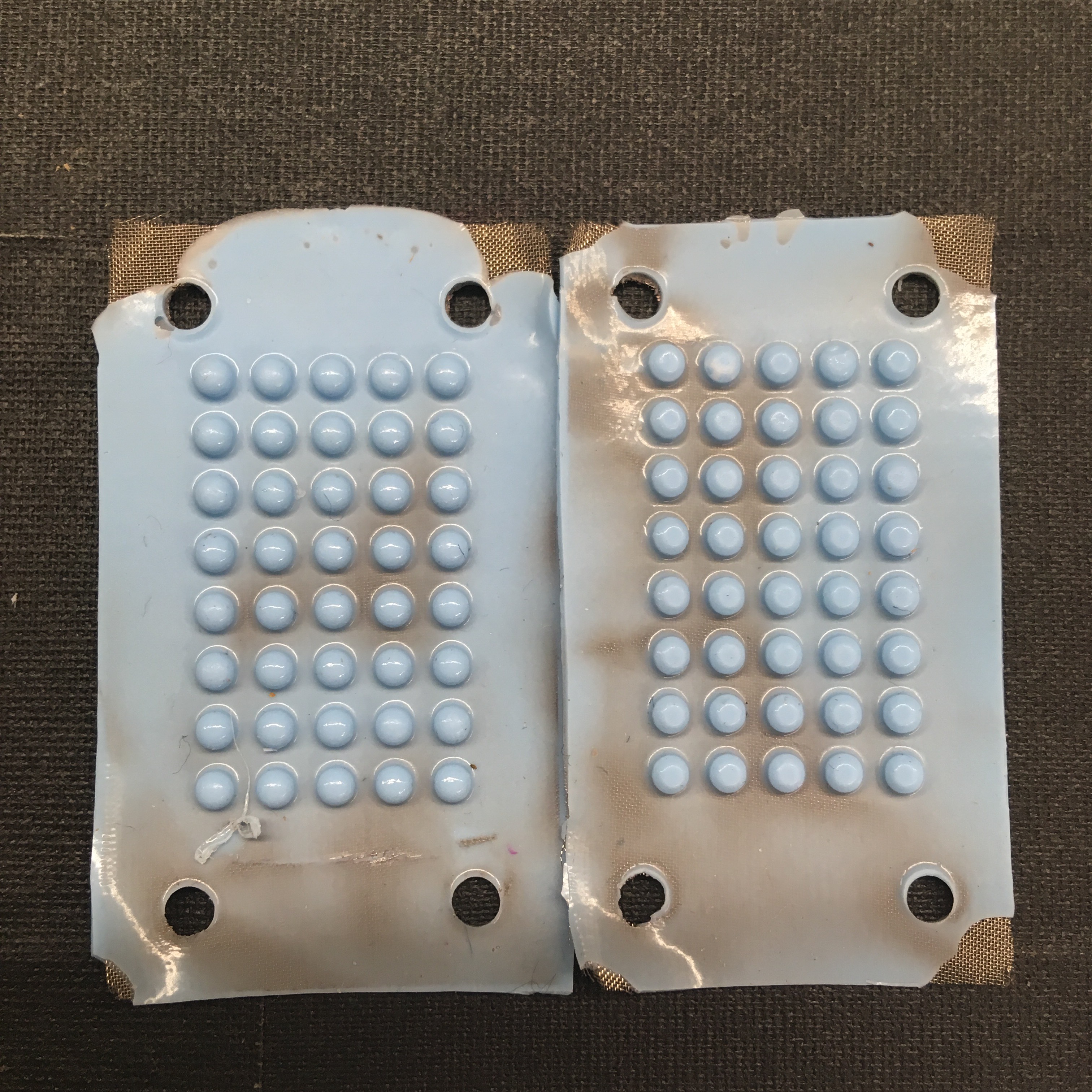
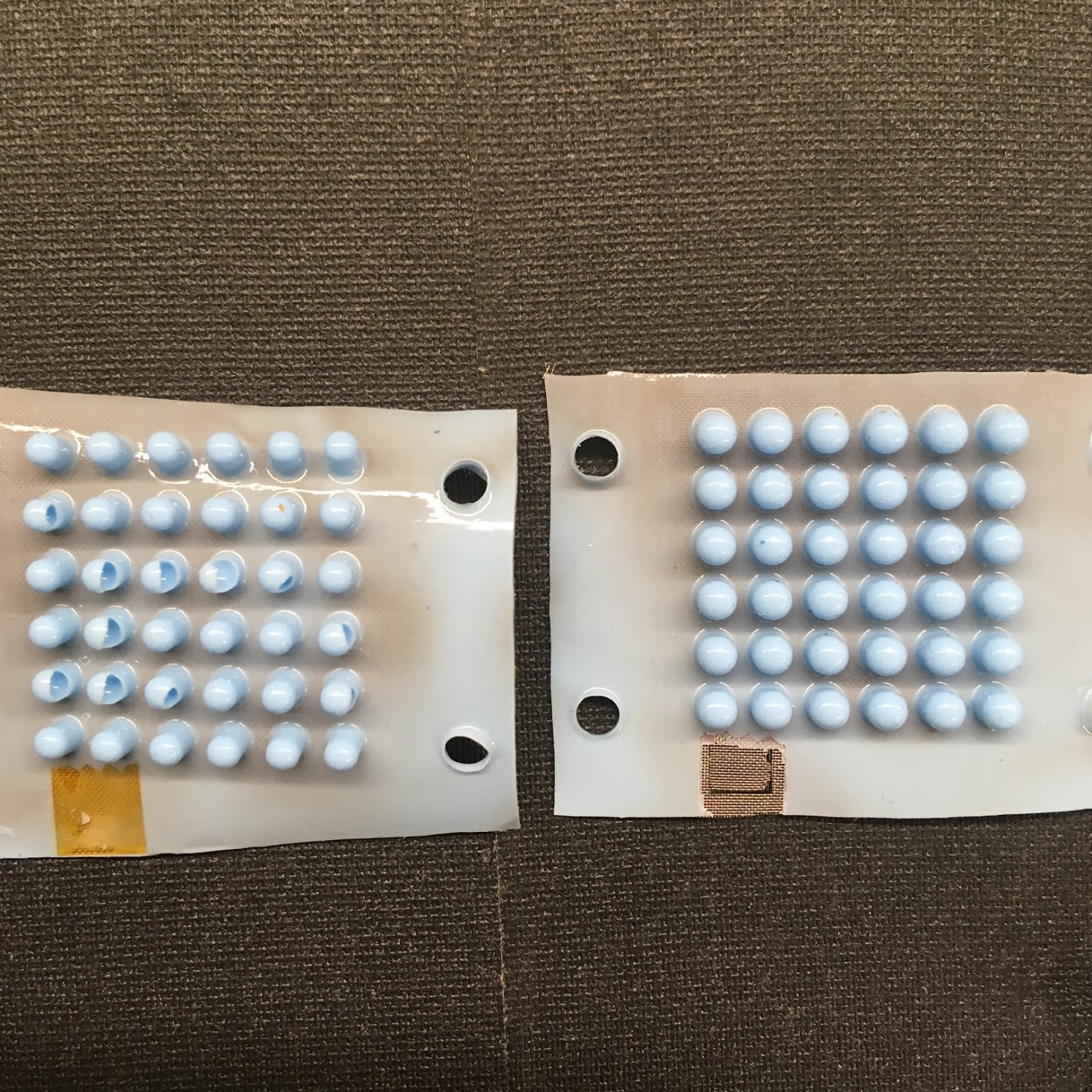
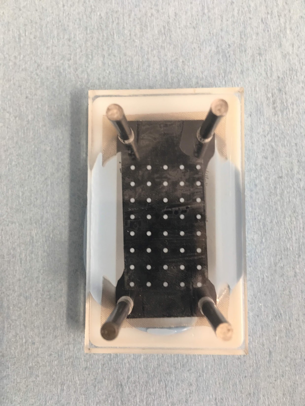
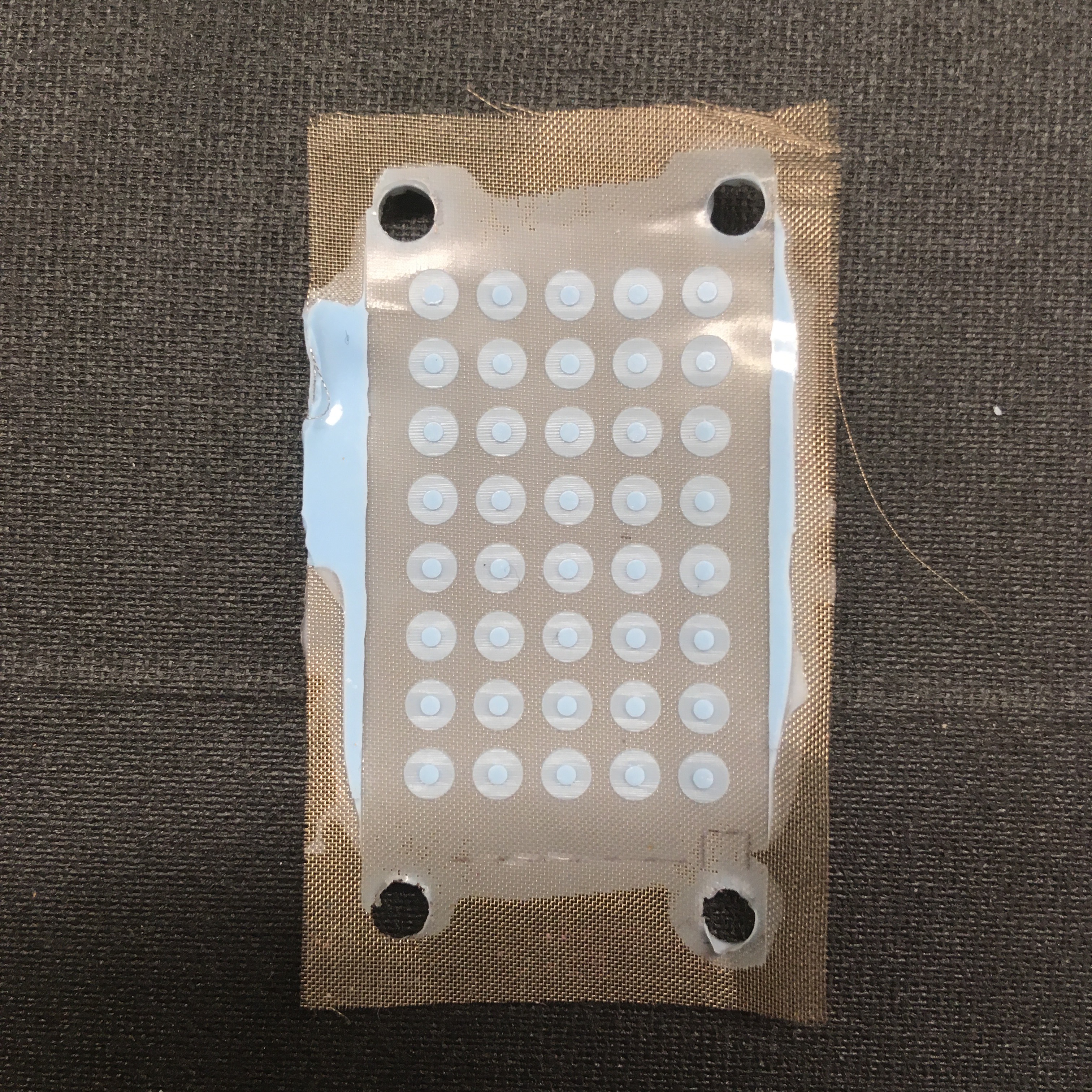
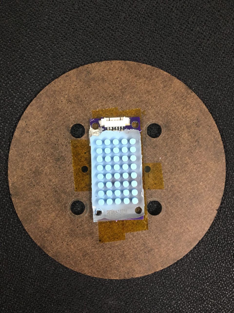
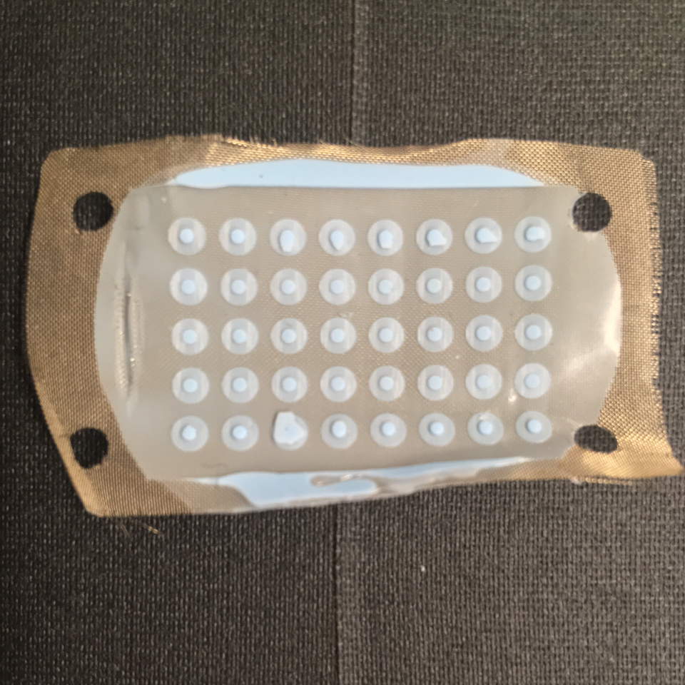
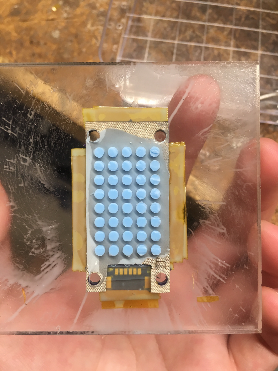
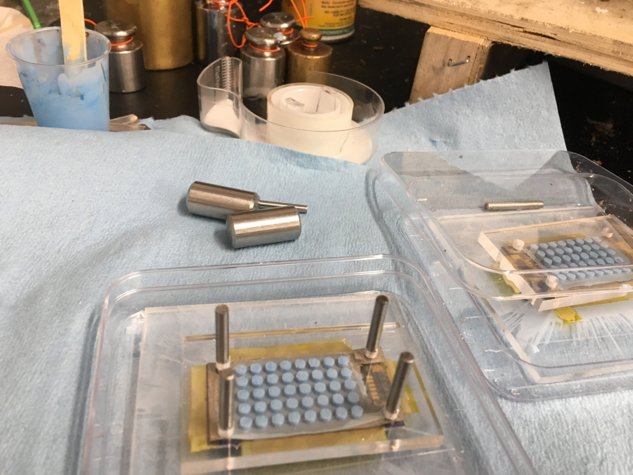
It's my last day at BDML! I was excited that all my molds from yesterday came out PERFECTLY which made me feel a lot better about finishing up this week now that I have workable samples for round-top and flat top 0.09" and 0.110". Today I worked on refining my fabrication process sheet so that the methods could be reproduced and I also prepared a final spin coat for one of my successful molds from this morning. I've learned a lot this summer and I'm really grateful for everyone at the BDML lab for contributing to this valuable experience. Also, here's my poster! Thanks for a great summer BDML!
August 21
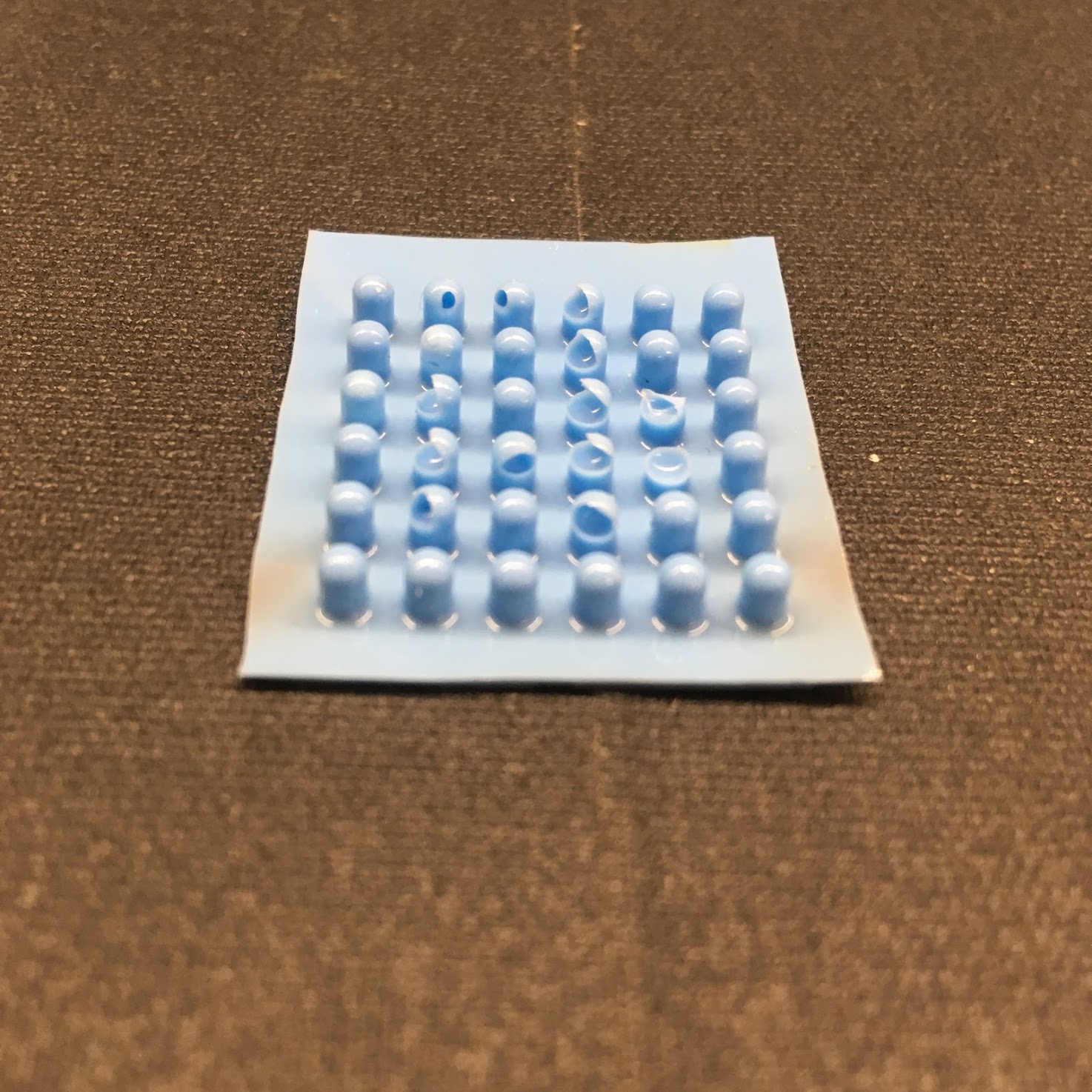
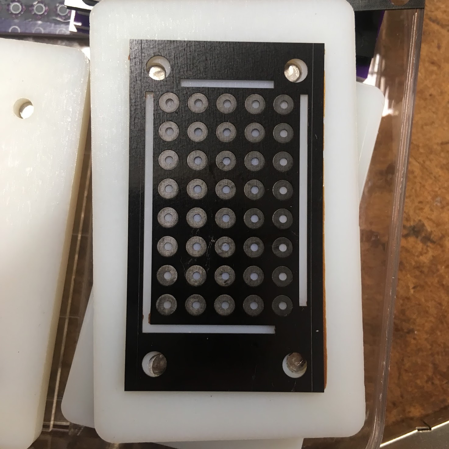
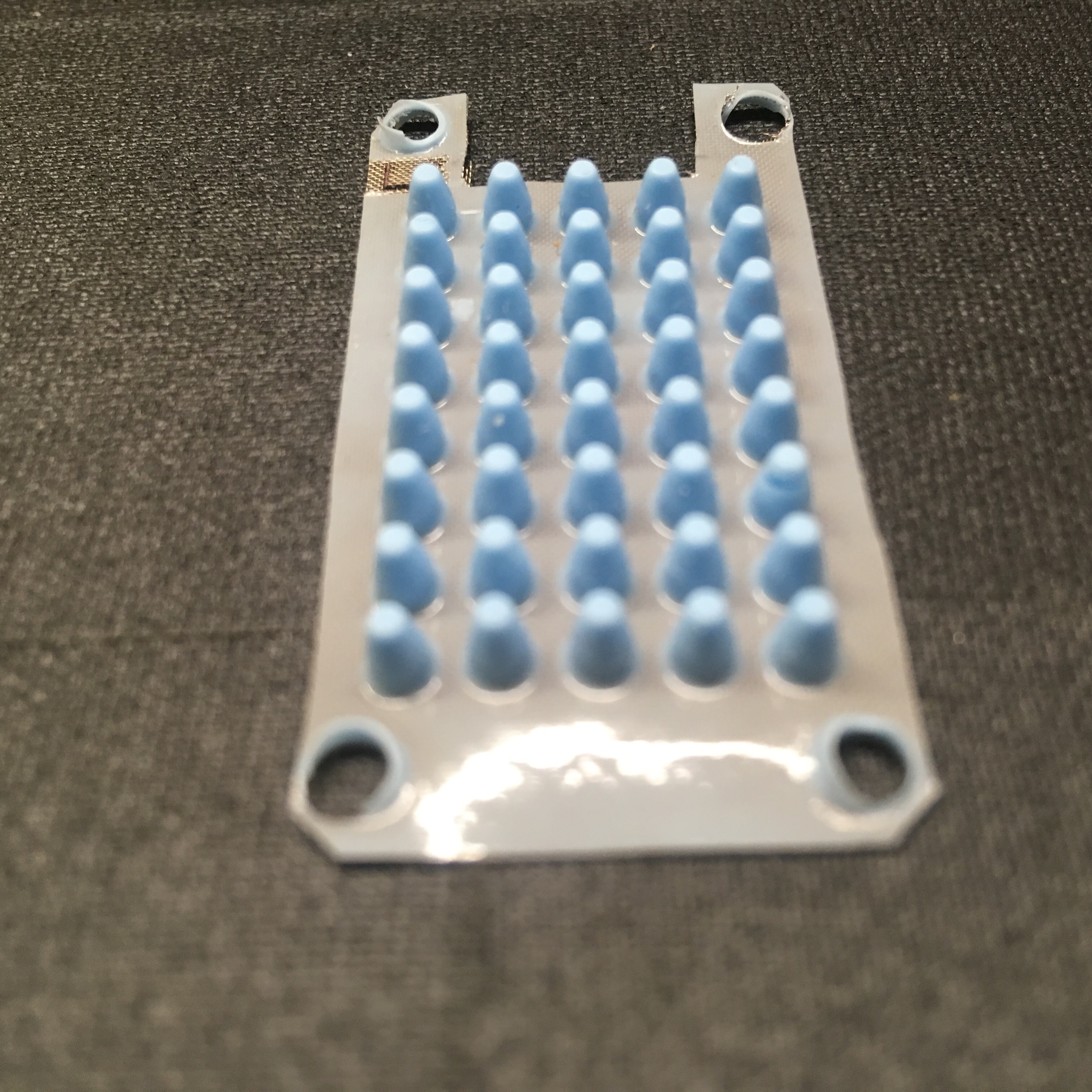
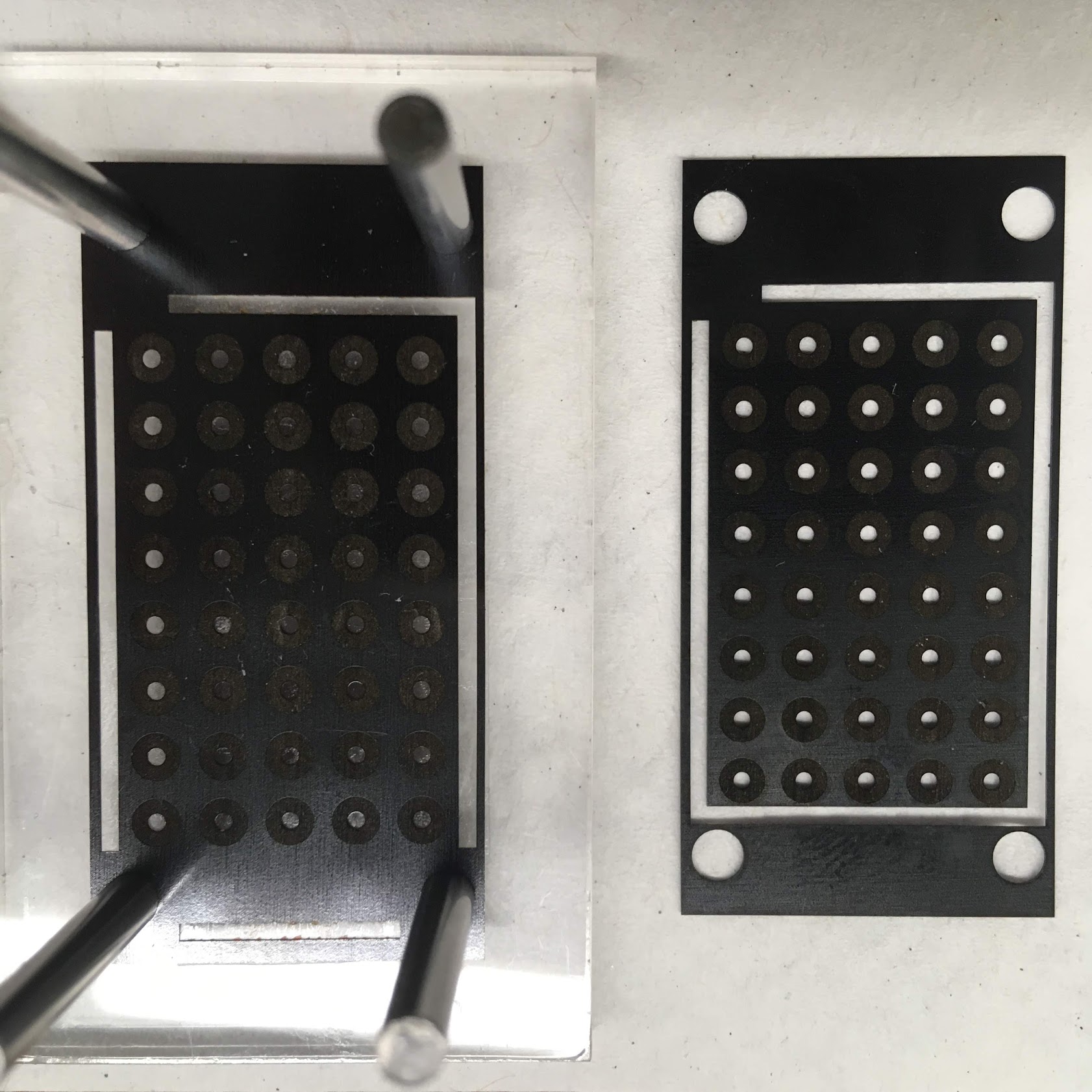
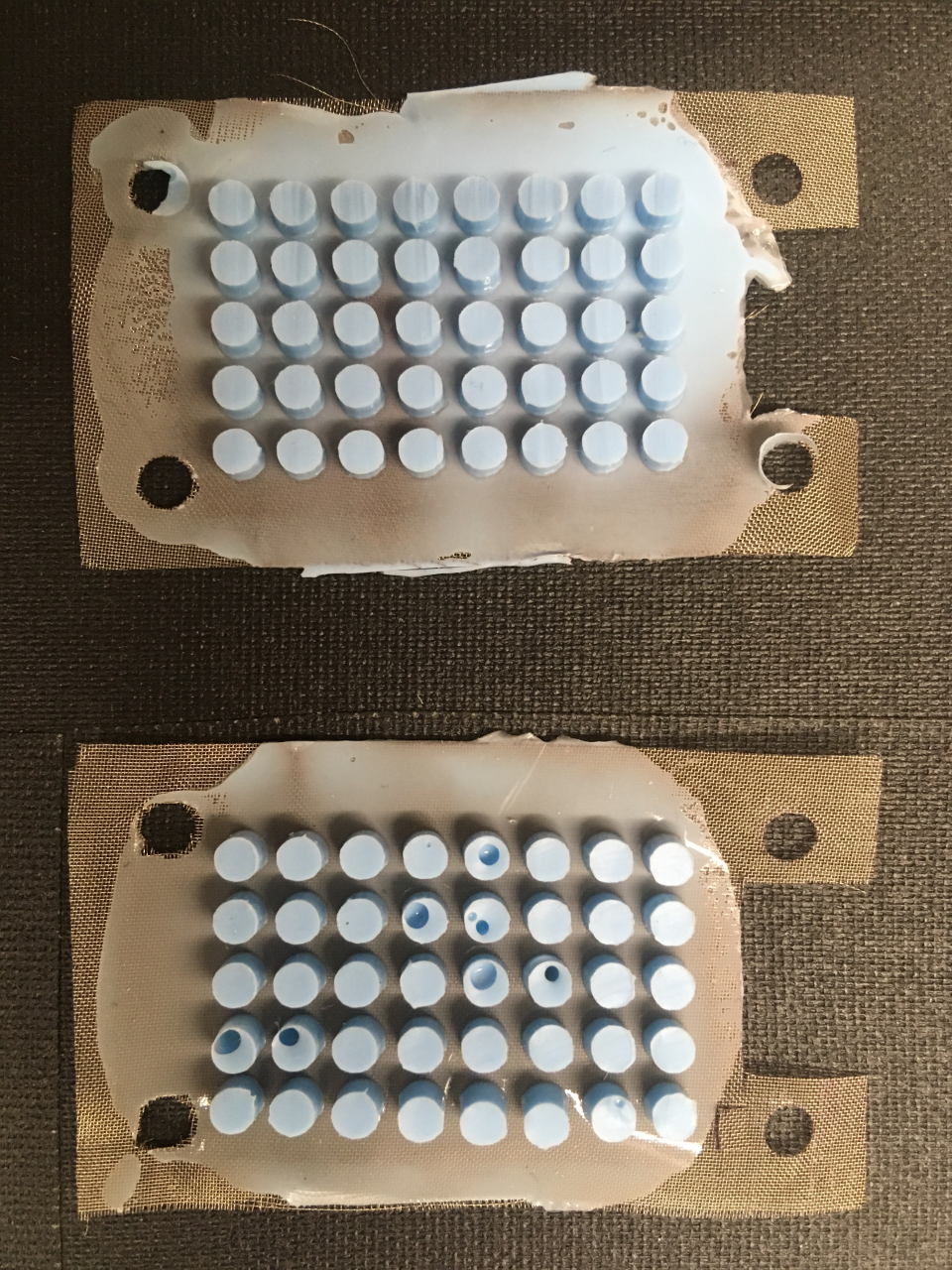
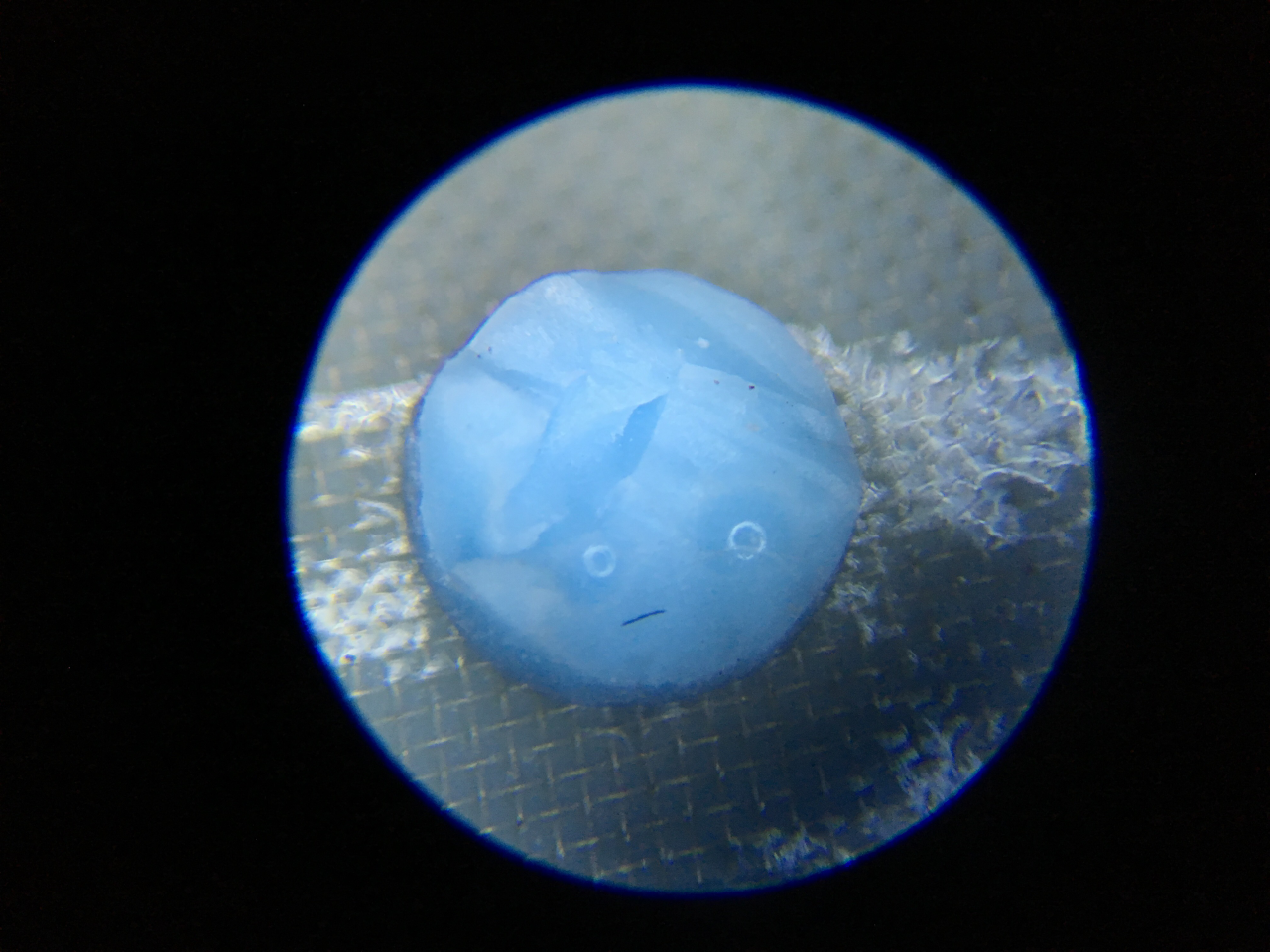
Today I cut more fabrics on the UV laser and another Kapton mold because I tore another while cleaning it. Round top molds did not come out, but because I had already made two molds before them, I was not able to use the needle that I wanted to use. I did the molds over again with the needle I wanted today. Additionally, I'm trying to come up with a little sample plate that I can use to show all the types of nibs that have been iterated over the summer. Within my collection, I have nearly perfect samples of all of the geometries and heights and so I think it would be a cool addition to my poster presentation. Things are winding down for me, but I am really anxious to get a round mold sample ready. I'll the molds waiting for me tomorrow. If they don't come out, I'll try again tomorrow.
August 20
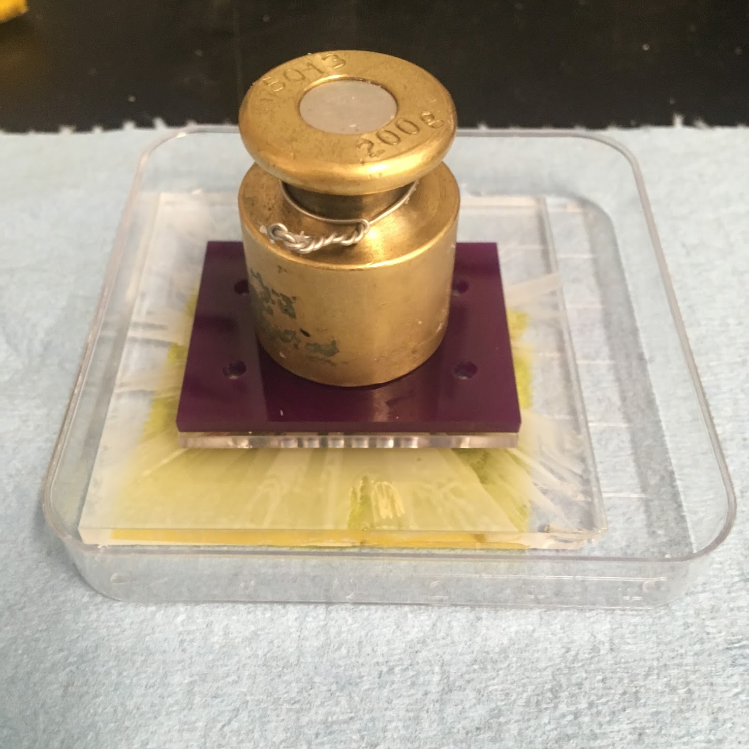
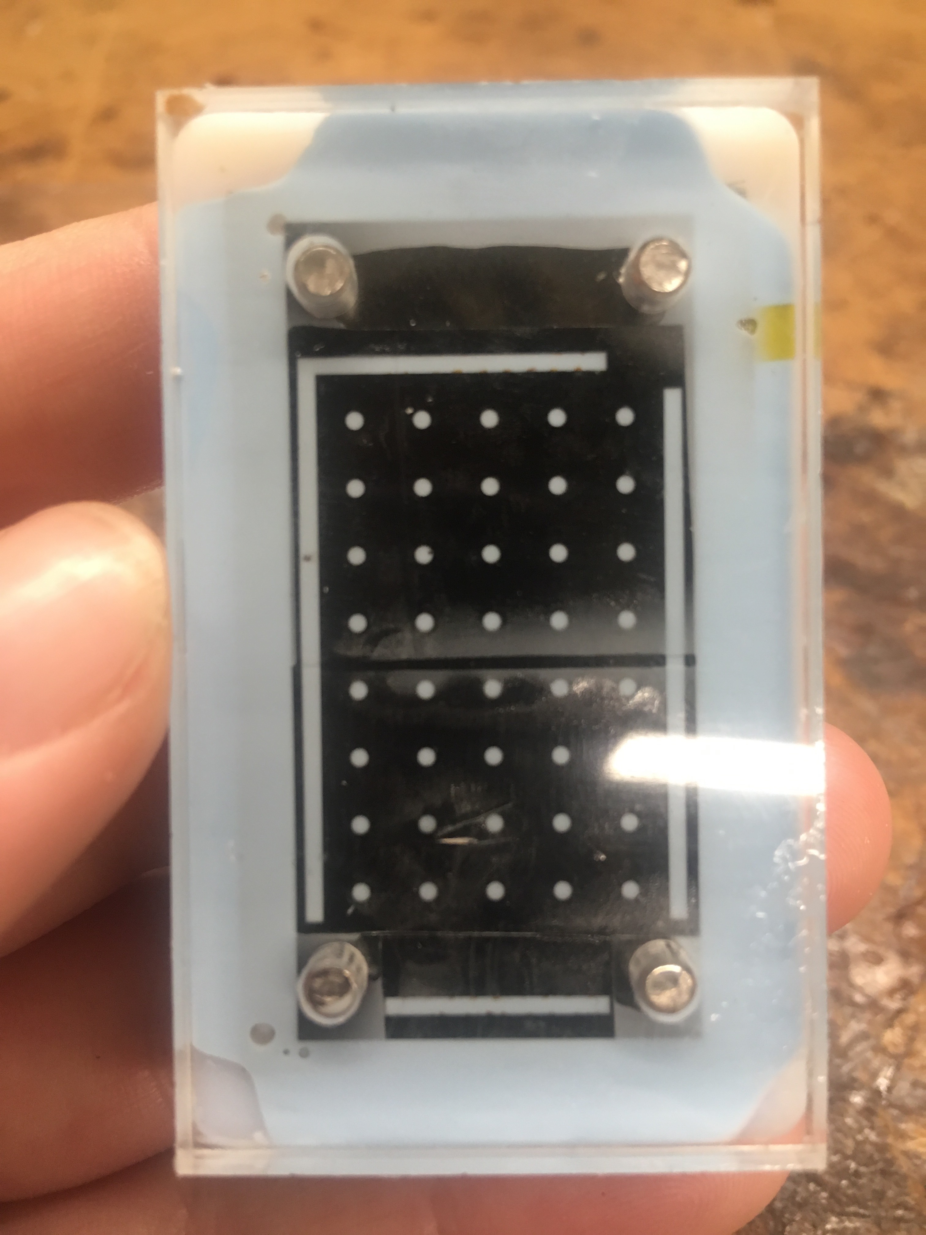
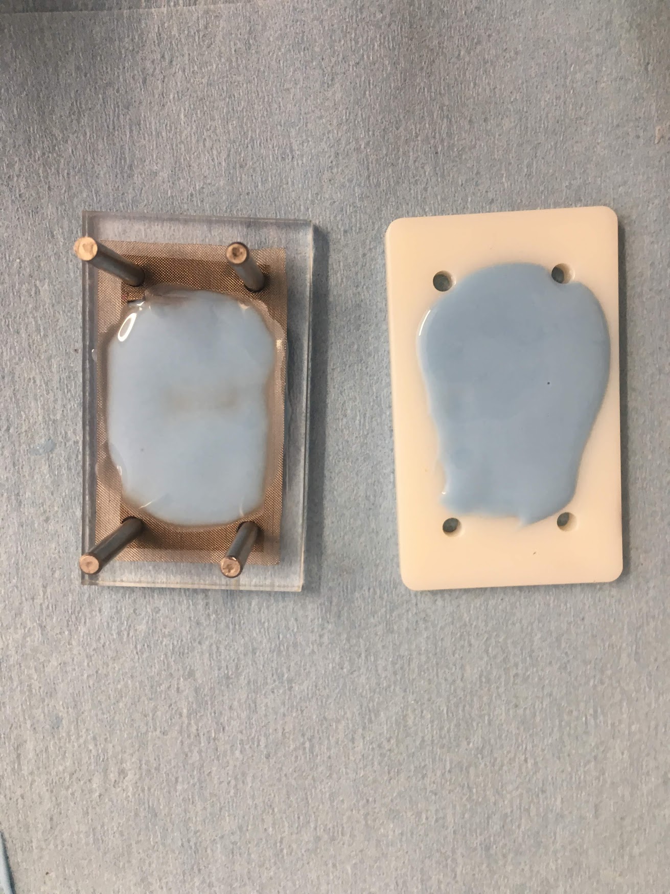
The spin coat and flat top mold from yesterday came out perfectly. I used epoxy on the connection flap and the sample was ready to go. Additionally, to salvage the PCB fail from yesterday, I sanded the spincoat off with 400 grit sandpaper and used IPA to clean the residue left over. The purple insulation that covers the electrodes was sanded off completely, but Tae explained that silicone spin coat itself would act as a new insulation. Next, I started two molds for two 0.09" flat top molds since I already had two acrylics. While those were curing, I spent sometime finishing up the poster and printing through Lathrop (YAY.) It feels good to get the poster done so now I can really concentrate on finishing up my work here before its time to leave.
There was some user studies in the lab but I was able to squeeze in a spin coat for the second 0.110" flat top mold. Finally before leaving, I prepared the molds for 0.09" round top and the 0.110" round top. Hopefully they come out!
August 19
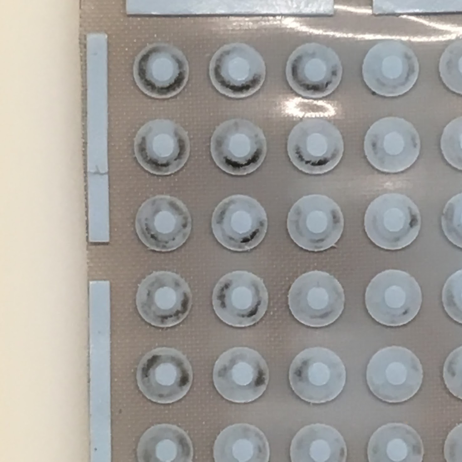
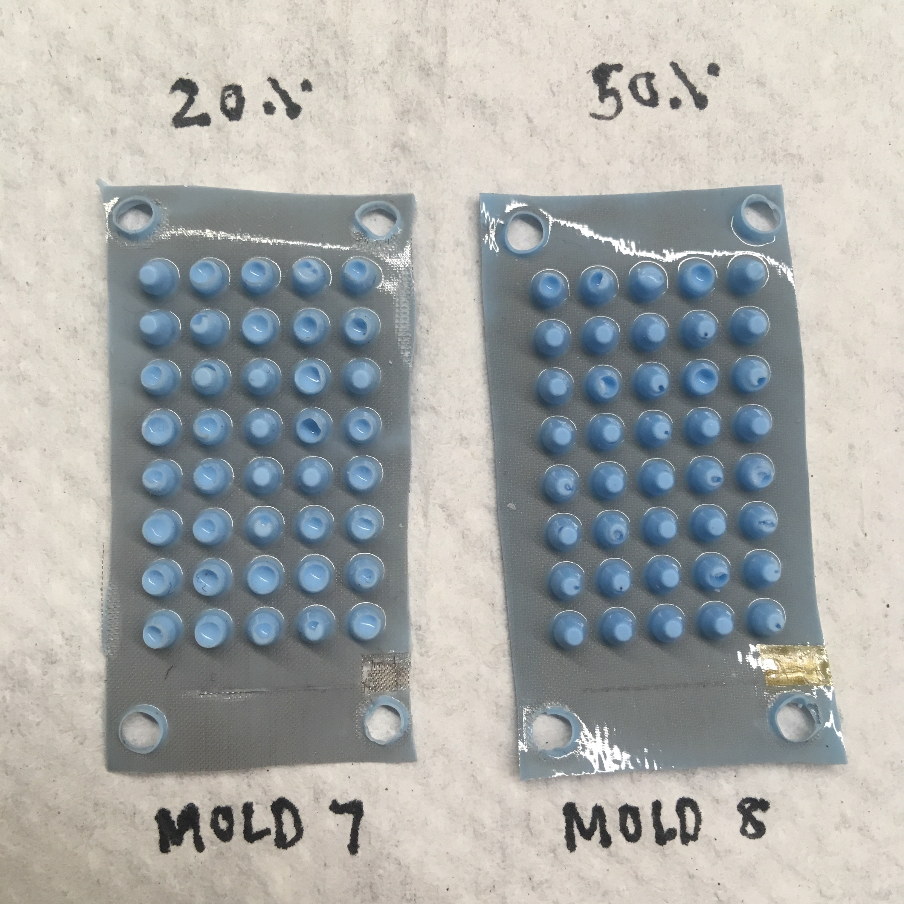
Last week! The molds from Friday all turned out perfectly in terms of minimizing bubbling, however I misaligned one of the molds (annoying) and will have to redo it. However, we have a perfect flat-top mold. The spin-coated PCB mold from Friday either slipped or was bumped because a whole corner of the PCB was not adhered to the board. The silicone could literally be peeled off. My goal for this week is to produce two testable samples for the 0.09" flat top and round tops and the 0.110" flat top and round tops. As such, I spent the rest of the day priming fabrics and making a flat top 0.110" mold (this will be the 2/2) and a round top 0.110" mold (also a 2/2). I won't post pictures of those because I think the photos aren't particularly new at this point.
Spent a lot of time doing finishing touches on my poster and in particular I focused on making the graphs more readable and easier to interpret.
Week 9
August 14-16
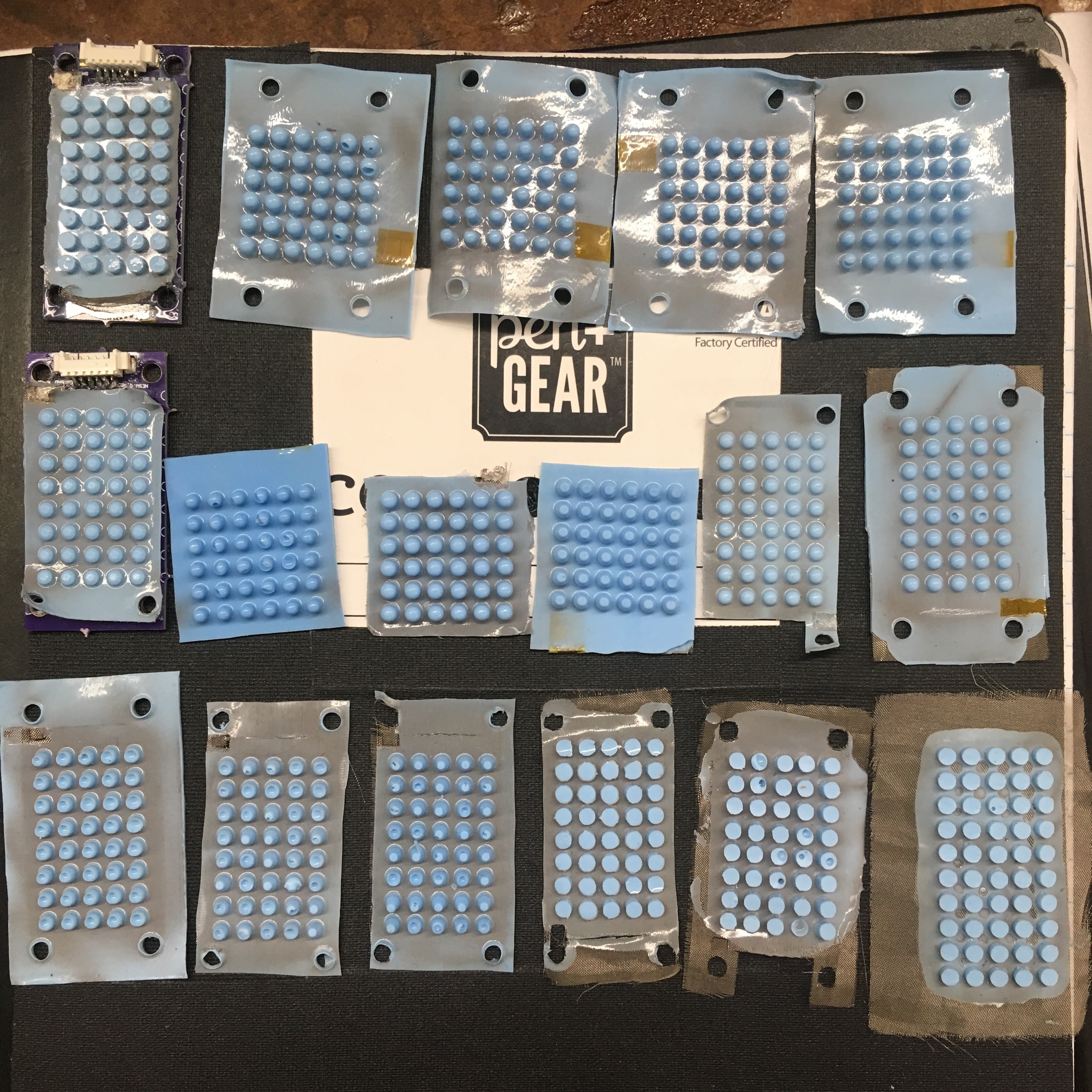
Just a funny photo of all the failed samples
This week has been a little crazy as my staffing job wraps up and as the SURI poster session approaches, so I�m grouping the past two days together. Back at the lab, my main goal for this week has been to successfully fabricate the 0.90� round-top nibs. During the sensor meeting on Wednesday, Ho Jung presented a new development in the testing of the sensors. While the pencil-top nibs detect slip vibrations better than the flat-top nibs, the pencil-top nibs compress irregularly (probably due to the limited amount of material at the tip) and therefore produce irregular normal force readings. This is not a problem we see for the flat top nibs, which are comparable to the ATI sensor. For this reason, there was more urgency towards fabricating a testable round-top sample.
Bubbling present on surface and base of flat tops
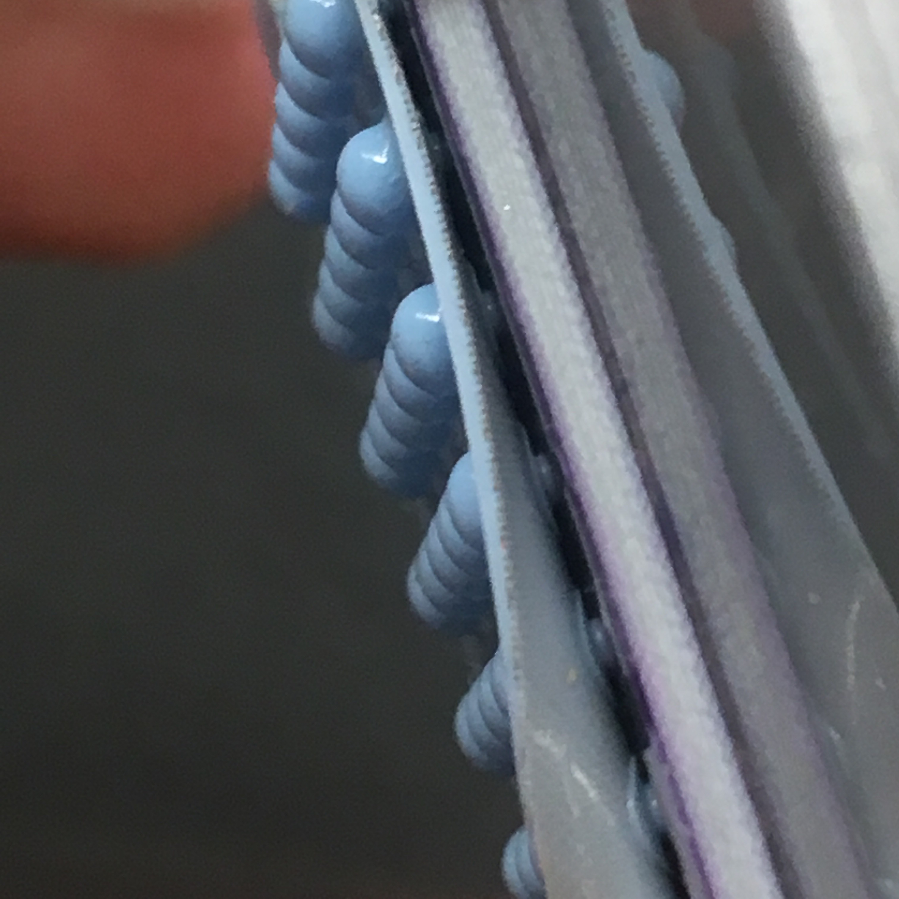
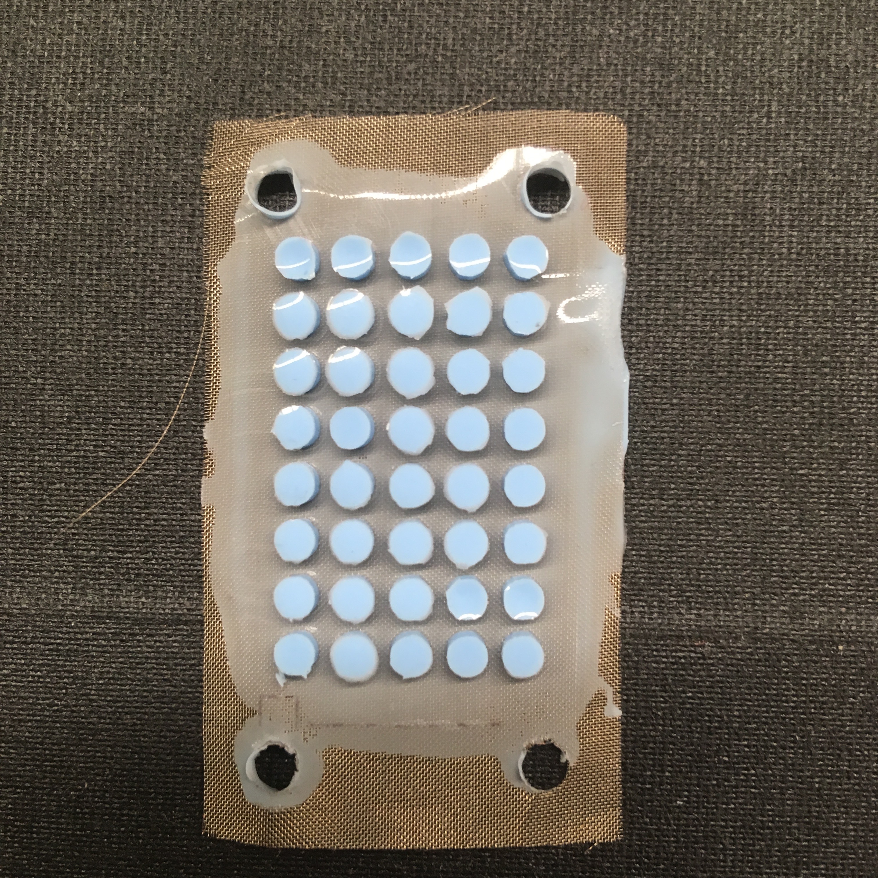
New Kapton molds are working well for yolks!
Since there was also a need to return to the flat nib geometry, I cut some new acrylic molds at Room 36 (0.05� tolerance to account for the acrylic/laser-cutting discrepancies for through holes). I had to refer back to my summer blog to remember the casting process with the acrylic molds, so I was not particularly surprised (though of course still disappointed) when the molds had significant bubbling. For future iterations, I want to use the larger needle with the acrylic flat top molds and flip them so that the molds set upside down just as the 3d- printed molds do.
To increase productivity, I�ve been trying to cast 3-4 molds a day. This means that if I have two molds of the same top geometry, I�ll mix silicone twice and apply to one while the other is in the vacuum. However, the quality of my samples seemed to degrade. At first, I thought that perhaps because I was using the very last bit of material in the Tap silicone supply that maybe that�s why my molds appeared to be getting worse. I don�t think this was the case. Either way, my next idea was to try a needle with a lower gauge (a larger diameter) in the hope that it would be easier to control the flow of the silicone. My hypothesis was that with the smaller needle, I could be more precise, but it required more hand pressure to keep the flow constant. I was not very good at it. I was genuinely surprised by how easy it was to push the silicone through the larger needle.
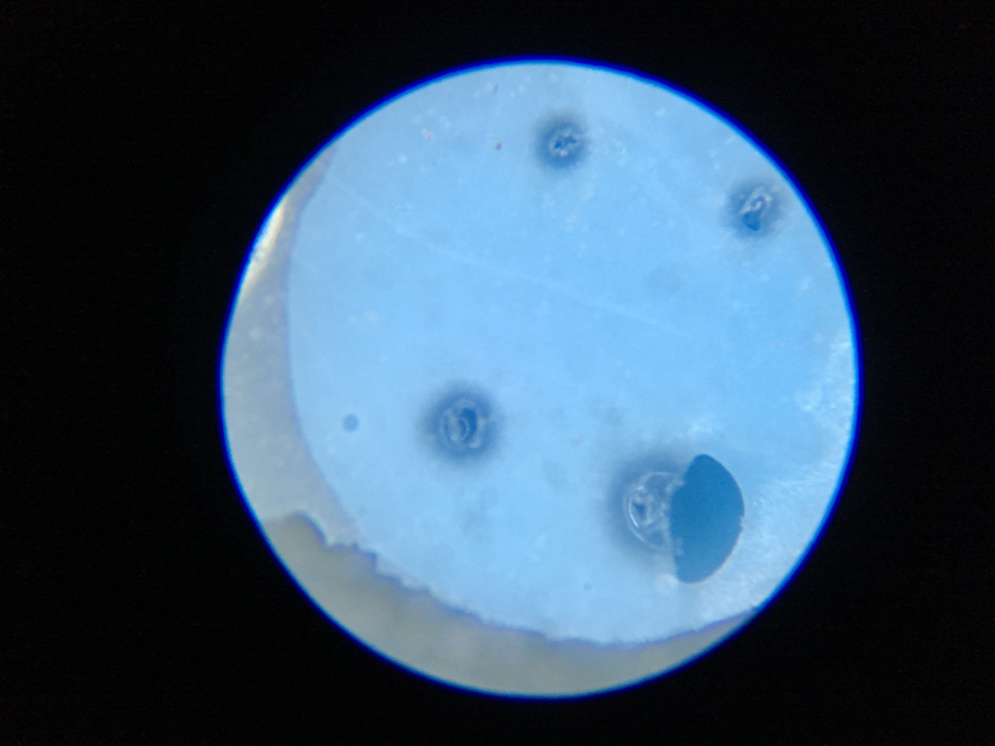
When it came to check the needle injected mold, I was excited to see the 0.09� round top mold come out perfectly (YAY.) Additionally, I checked the 0.110� mold that I had spin-coated onto the new PCB and the nibs appeared upright and intact. This is a good feeling especially knowing how little time is left for me to work on this project. I prepared more fabrics and another PCB to make a complete, testable 0.09� sample and to apply the needle method with the flat top molds.
Working on my poster has also taken much of my time this week, both with formatting the poster itself and designing illustrations/taking photos that I want to include. Presenting the poster at lab meeting gave me a lot of feedback to work on, but I feel like I got most of the work done already and I�m satisfied with that. I�ll post a photo of it when it�s finished because I found it helpful to see past SURI posters on their summer blogs.
August 13
So. The first sample for the new PCB design does not work as expected. When Tae cut the silicone part of the PCB, we saw that the pillars had flattened out over the PCB electrodes, rendering them useless. We have several theories as to why this happened. First, recall that during the spin-coat process we had to reduce the speed to 4000rpm because we could not achieve the full vacuum due to the cutouts in the acrylic. Second, we added a 200 gram weight to the top of the spin coat while it was curing, while in the past I�ve been only covering it with an acrylic and applied no weight. Finally, we realized when comparing the �yolk� height of the previous silicone design and the current design, the yolks appeared shorter in the new design. This would mean that the nib column (white part of the egg relative to the yolk) was more are risk of curing onto the spin coat.
A deeper etching appears more red under light
For this reason, I spent my morning back at the UV laser cutter to make a mold with a lighter etching, thus allowing the yolk part of the design to be taller. We�ve learned that the UV laser cutter can be somewhat inconsistent but holding up the Kapton to the light to simply compare relative depth of the etching can be helpful. I spent time finding the focal point of the laser and then experimented with tweaking the settings like the laser speed and the number of passes. I ended up settling with these settings: focal point at 6.15; etch: 500mm/s and 10 passes, crosshatch 0.60; cut: 120mm/s and 25 passes (adjusted because not all of the previous cuts would go through, and I would have to manually cut them with the blade.) The new molds appear to be better, though after bringing them back to the lab and comparing them, they looked very similar to the previous layers until I put them up to the light. I suspect it will easier to tell by the silicone mold that is produced from this new layer. I prepped for two molds (although I did print four Kapton layers) in case I want to make an even thinner etching tomorrow morning based on what the yolks look like.
On my todo list is to go back to the PRL and make new acrylic spin plates with only the cutouts for the circuitry and not for alignment. Additionally, I want to use a thinner acrylic sheet so its lighter�maybe around 3/16�.
August 12
Note the thickness of the silicone on top of fabric
Bubbles ):
Today was a productive day. First off, we have our first sample for the new PCB design! It hasn�t been tested yet, but so far appears that the thicker spin coat has not greatly affected the mold, although its harder to tell the condition of the yolk/nibs with the border design in place. As for the molds I squeezed in at the end of last Friday, one of the weights had fallen to one side and so that mold has a thick layer off silicone on one side. This will affect the structure and sensitivity, so I won�t be using it. However, all the pencil-top nibs came out so that is promising. The 0.09� round-top nibs did not come out (again), more brainstorming required. Most of the morning I spent at the UV laser cutter in order to print more of the Kapton molds. I figured out a way to align the etch and cut drawing without having to invert the fill setting (in other words, previously was manually centering the etches of the mold relative to the cuts of the mold, and in one of the molds this was quite noticeable.) Another note, a preset option when you import a DXF file is to �fill in polylines� for some reason unless I manually opt out of this setting, the software doesn�t fill all my sketches. In the end, I managed to print three Kapton molds (I had inadvertently ripped one of the previous ones while removing the double-sided tape.) I also cut 10+ fabrics so that I would have a steady batch at hand. Now, in theory, I could make four molds in a day.
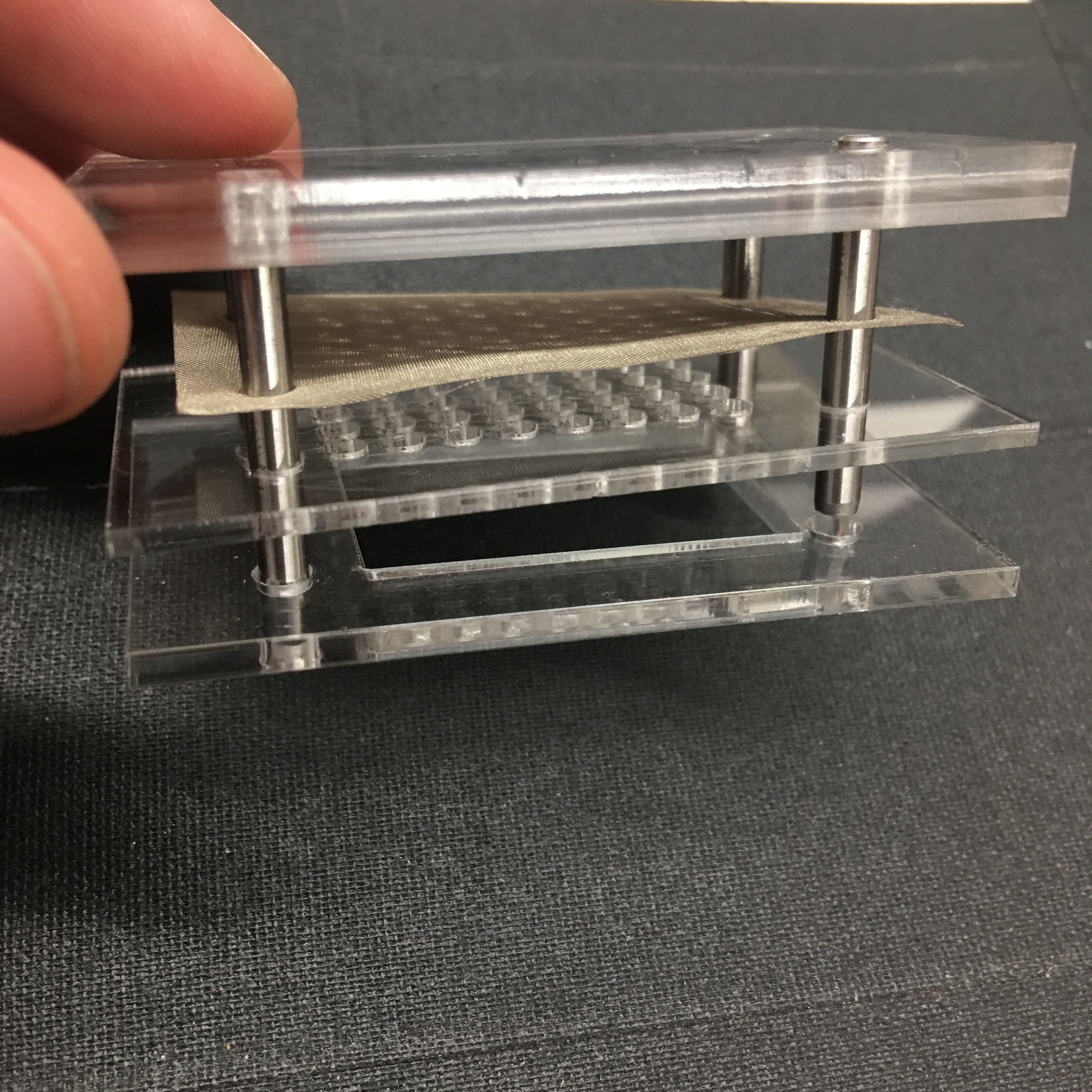
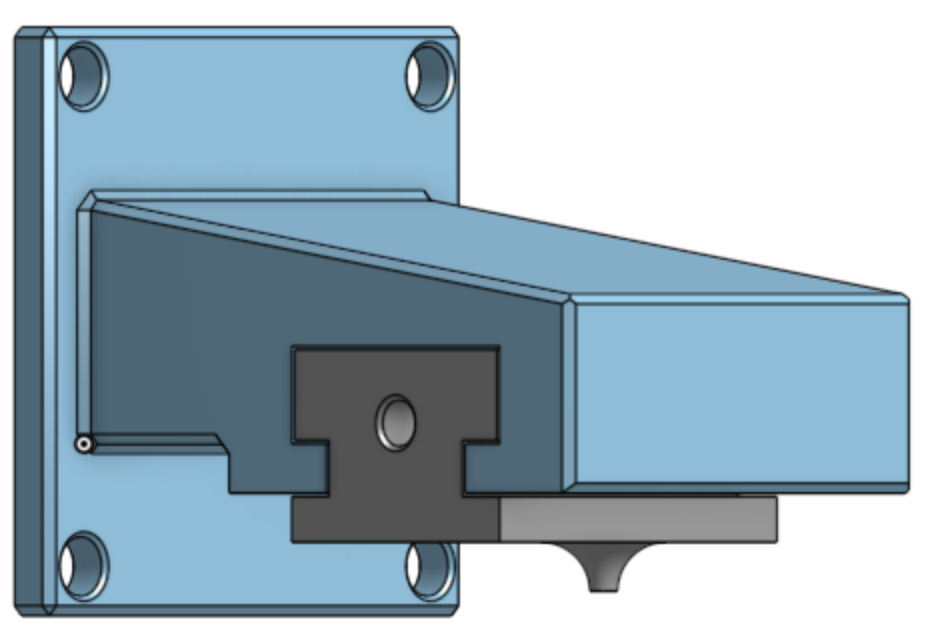
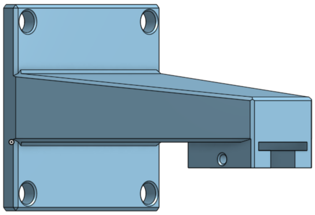
Another objective I had today was to make an updated Duron mounting plate for the test-set up. The current model was too thin and did not allow the new PCB to lie flat because of the circuitry on the underside of the board. I made a new design with the same cut-out as the PCB board and added one pair of the alignment holes that would not interfere with the tightening bolts. I used �� Duron and after adding the one completed sensor we did have I was pretty happy with the result. One set of the alignment posts on the PCB had to be removed for the tightening bolts to not interfere.
Before I left for the day, I prepared two molds � the 0.09� round top and the 0.110� round top. I�m little lost as to how I can improve the 0.09� round top mold, but this round I did try poking each nib after the second round of degassing just to see if that helped eliminate the bubbles that are persisting. I�m really not quite sure how to improve beyond that. I�ve also begun to start thinking about my poster and what pictures/drawings I want to make for it and the paper.
Week 8
August 9

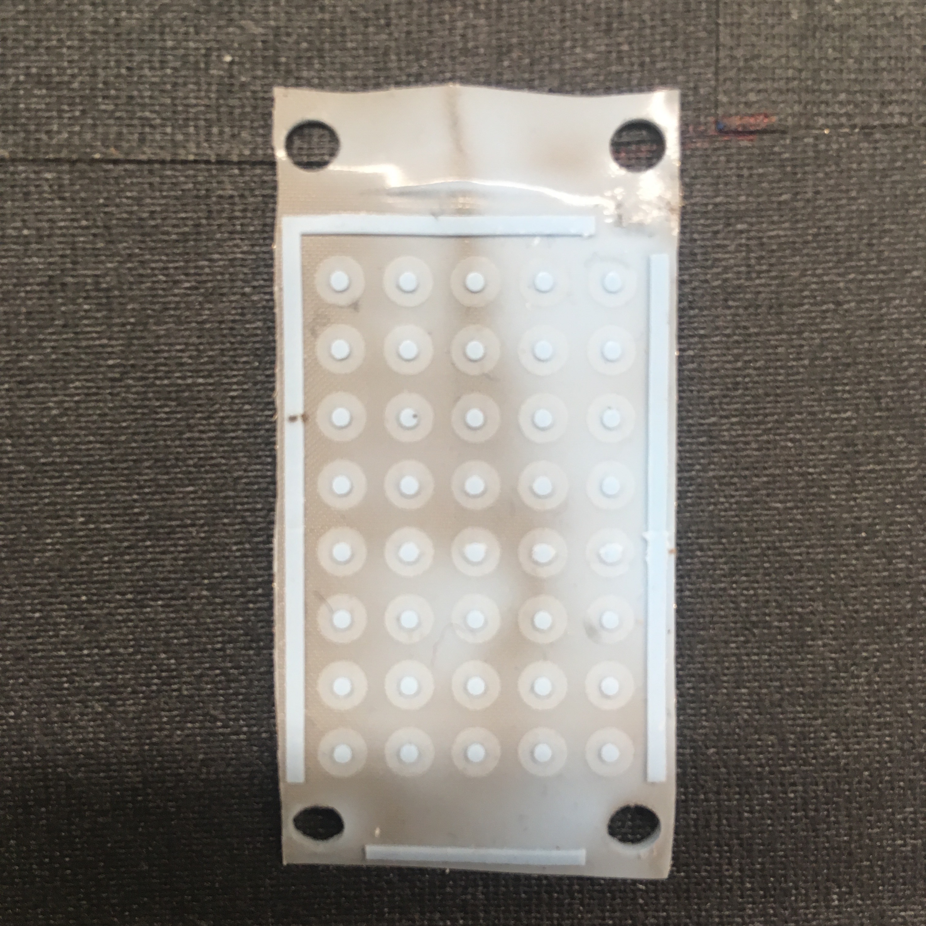
Left: 0.09� round top, Right: 0.110� round top
Close-up of debris leftover from Kapton layer
The new molds were finished today and came out with mixed results. The 0.110� mold seems to be nearly perfect (aside from some residue Kapton ash that stuck to the bottom � note to self: clean Kapton more thoroughly with IPA after UV laser cutting.) The 0.09�, however, had significant bubbling even though I used the same process and fresh silicone. I think I will have to brainstorm on this because the �injection� method has proven effective until now and is already a difficult step to work with. Either way it was exciting to have the new molds come out and I went forward with the 0.110� mold as Tae had a prototype PCB that I could spincoat.
Perhaps a different type of tape would seal better
Applied a 200gram weight
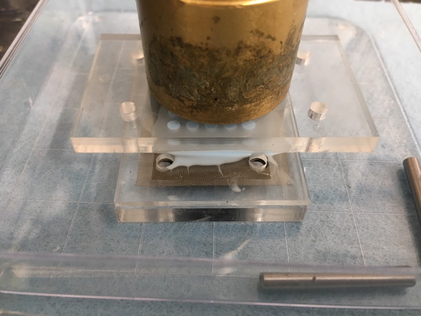
This is where it gets interesting. Spincoating the new PCB will require some significant troubleshooting. At first when I laid the acrylic plate with the PCB on to the wafer spinner, I did not realize that the vacuum had not reached its ideal pressure (~25 psi) as it normally does. Thus, of course, the PCB flung off. When I did realize that the pressure was lower than it should be, I tried to see if there was a leak or I had incorrectly locked the air valves, but everything checked out. I asked Tae for some help and we realized that the cutouts on the bottom of the acrylic were preventing the vacuum from forming between the wafter spinner and the plate. We tried covering it up with Kapton tape but could only get the pressure up to ~21 psi. Because the silicone was running out of pot-time, we spun at 4000rpm for 1 minute and got a workable spin-coat layer. Afterwards, we added a 200 gram weight. I am curious to see the results from this, but I am hopeful. However, for future samples I do want to find a way to get the rpm up to 5000.
Today was lab meeting. Mela got some critique on her poster for the SURF poster session, and I realized I should probably start thinking about what I want to talk about/put on my poster.
August 8
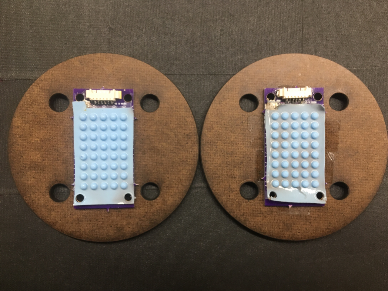
Yolk design no longer visible when lifting up silicone
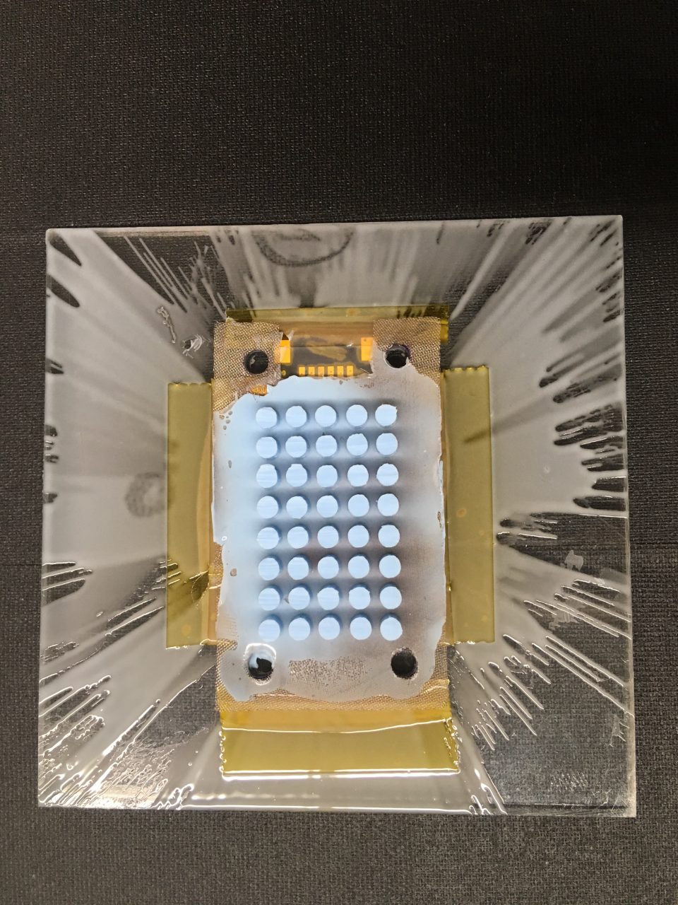
The border design worked well with the old PCB. The border adhered to the spin-coat well and when moving a finger across the nibs, the fabric does not wrinkle or lift from the PCB at all. Of course, after a full round of testing, we shall see if the design is as robust and it feels � but the results so far are promising. I soldered the connections to the pico molex (getting better at this) and applied the silver epoxy to the fabric connection flap. I made sure to trim away the excess silicone/fabric to be entirely clear from all electronic connections to prevent the shorting problems we experienced on the last sample.
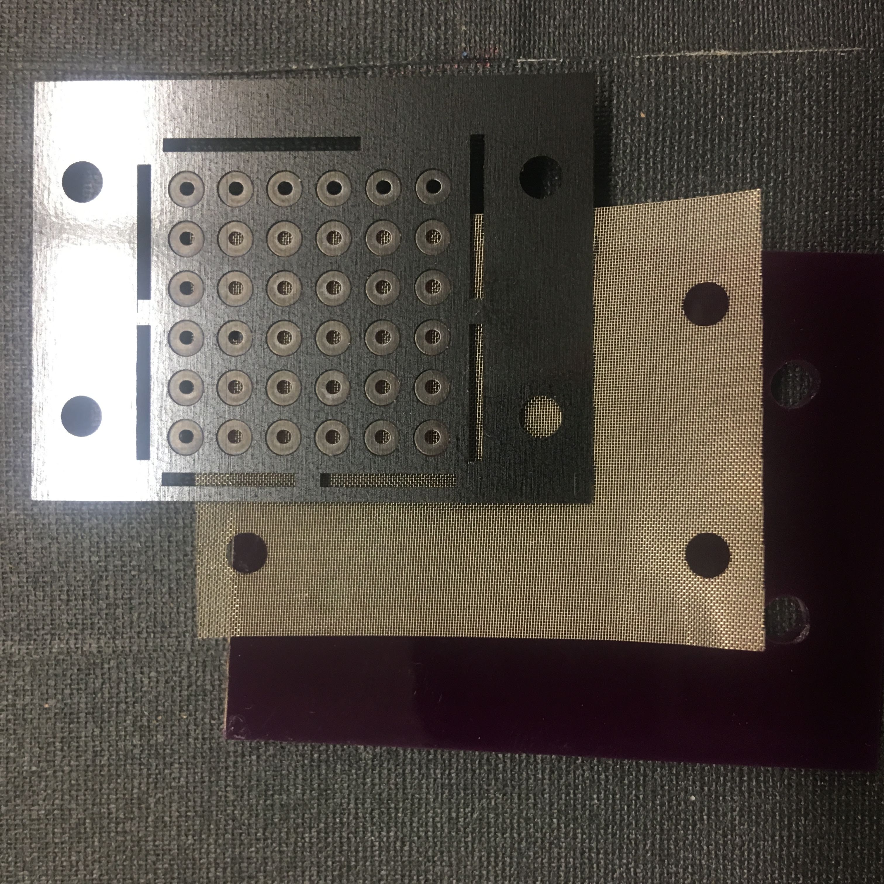
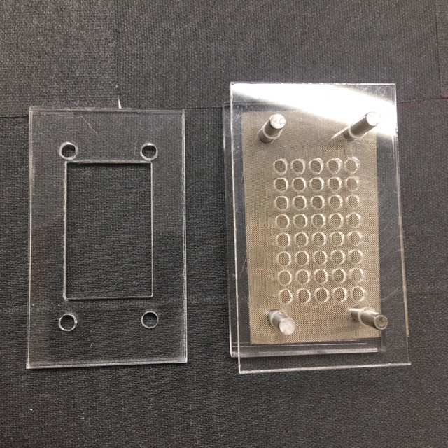
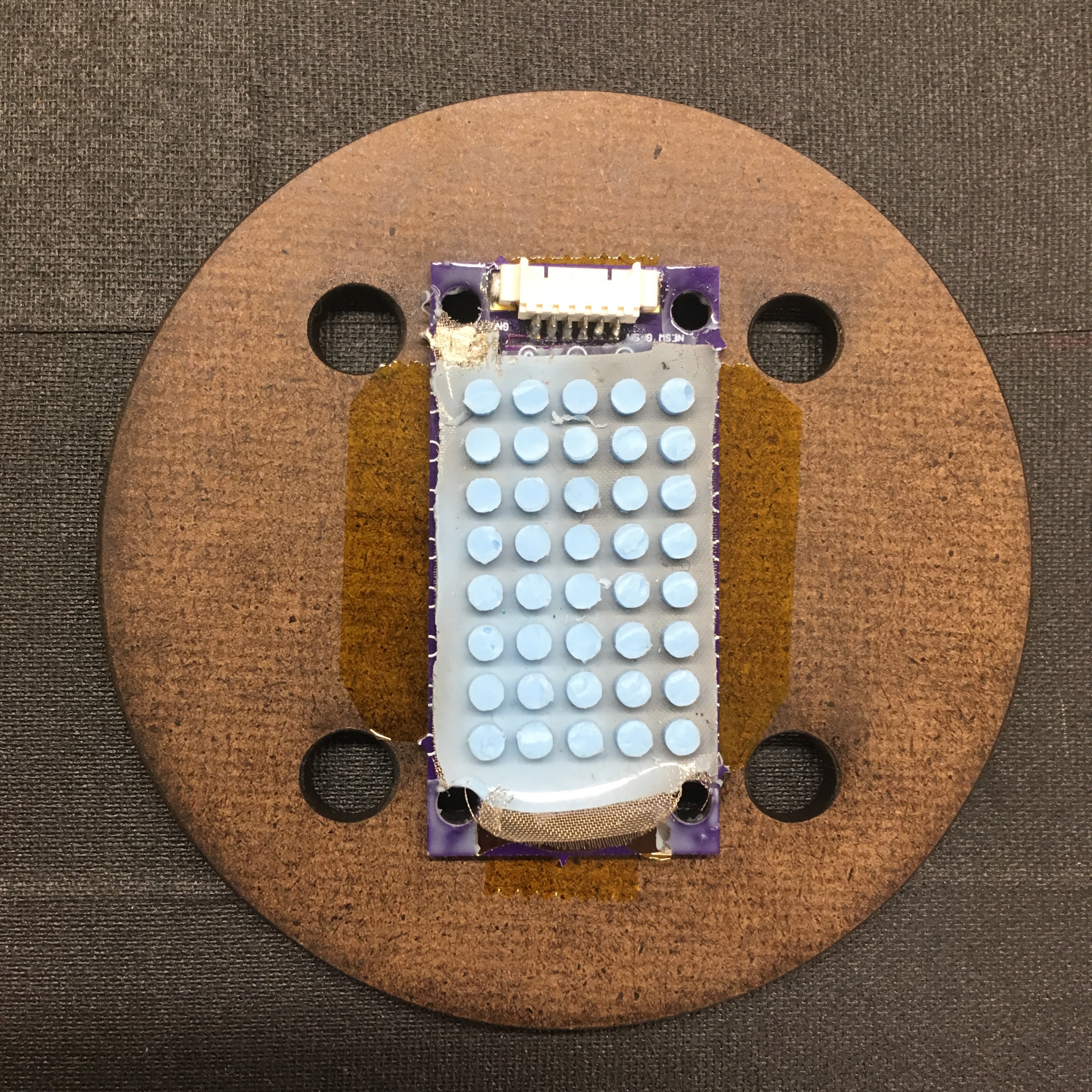
Yesterday I was ill, so I did my best to catch-up and make a lot of progress today with the new molding process now that the new PCBs had arrived (they look like little critters). I went to Room 36 very early in the morning to cut all the parts that I would need in acrylic and duron for the new PCB. While I was cutting the duron test mounting plate, I realized I did not put in the holes for the bolts that mount the plate onto the ATI force sensor. When I added these to the design, they somewhat coincided with the alignments. I decided to prioritize the bolts and instead adding an etching of the PCB onto the duron to help with alignment. For the acrylic cuts, I made the base acrylic layers, spin-coat acrylic plates (which have large cutouts so that I can solder the molex prior to spin-coating) and some acrylic with holes to allow for placing the fabric onto the PCB.
New bottom layer, fabric and Kapton mold
After returning with these parts and looking at the new PCB, I realized I would need to adjust my design somewhat. For example, I made a cutout for the molex on the spincoating board, but I would also need one for duron mounting plate. Additionally, I accidently used a thinner acrylic plate for the base layer, and so the alignments slip and are a lot more difficult to place. Worth noting that for the 3d-printing designs (Which have a different tolerance for through holes than laser-cut acrylic) are undersized such that the dowels actually stay in the holes which I have found very helpful for alignment. For the next round of laser cutting, I will intentionally undersize the through holes to perhaps allow for a similar technique.
August 6
First thing in the morning, I checked the mold with the border design. It turned out well, and the injection method filled all the nibs even better than it did the first time. Worth noting the process I did just for confirmation: After mixing silicone, quickly apply on to fabric and degas material and fabric for 5 minutes. Fill up syringe (more will make it easier to inject, reduce pressure by pressing plunger without needle attached until silicone reaches bottom of syringe) and inject into mold (this will take a while.) Degas for 5 minutes (any longer will go too far into pot-time) and refill with syringe. Apply generously to top of mold and fabric before adding weights. I did not use mold-release, and it did not affect the mold.
I primed the PCB, and later in the day I did the final spin-coat step. Another note on this: because the borders are already 2mm in height and are so close to the edge of the PCB, there was no need to add a 2mm shim of Kapton tape around the whole border of the PCB. This was nice because that usually takes a while and is a little annoying to do, although I still used two layers of Kapton tape to cover the copper electrodes.
Meanwhile, I also spent a generous portion of my day with the UV laser cutter. I wanted to make sure I was getting the cuts/etchings I wanted for the new Kapton design for the new PCB design. It took a while to get the settings exactly how I wanted, but I think I got two workable Kapton molds for the new PCB. I added a numbered code to be etched onto the top corner of the mold to help me distinguish between the 0.09� diameter mold and the 0.110� diameter mold.
August 5
Today met briefly with Tae and Ho Jung to talk about the new sensor design. In particular, something I was struggling with was that for the new PCB, the NSWE electrodes form a diameter that is 0.13� wide, which is wider than the 0.1� diameter electrodes in the previous PCB version. When designing the molds, I realized this meant that the nibs would be clustered more densely on the sensor which would perhaps change the parameters of our experiment undesirably. We decided that the while the electrodes diameter changed, the silicone nib diameter did not necessarily need to match the electrode diameter. According to simulation, thinner nib diameters would stimulate better than wider nib diameters. However, a smaller diameter nib would be lest robust.
New Kapton mold for the old PCB design
This is something Tae wants to experiment with so I will now be making 4 molds. Pencil-top and round-top molds will be made all in 1/8� height. Each geometry will have a mold for 0.09� diameter nibs and 0.11� diameter nibs to test the sensitivity off the thinner nibs. Additionally, this would mean I would need two Kapton molds � one with 0.110� diameter etchings and another with 0.09� diameter etchings. I spent a good portion of the day editing my CAD files and sending the mold files to Sam to be printed on the Objet printer. With the remainder of my day, I also cut a new Kapton mold for the old PCB model but with the reinforced border cutouts. I then made the mold using the injection method with the needle syringe. The mold appears promising.
Week 7
August 2
Just one of the new molds I am working on
Today I spent most of the day working on the new CAD designs for the cluster PCB. For the new PCB, I need to redesign the 3d-printed molds, the acrylic base layer, the fabric, the Kapton layer, the Duron testing board, an acrylic cutout layer for placing the fabric onto the PCB, and a thick acrylic slab for the wafer spinner. Along with redesigning the mold to a 6x6 array, the position of the fabric connection flap and the molex are also different so these are things I will be considering in my design.
Also, in order to test if the boundary layer does help with adhering the silicone/fabric on to the PCB, I will also be cutting a new Kapton layer for the old design (since we still have PCBs leftover.) I spent a good amount of time making sure that Kapton would be more durable for molding. However, the UV laser cutter was reserved for most of today, so I wasn't able to get that done despite being ready with the design.
Soon enough, it was lab meeting. I actually really enjoyed listening to the medical robotics teams talk about their projects. I am not positive if I remembering this correctly, but I think there was machine/mechanical device that mimicked the pressure/rhythm/motion of a heart valve and that's what they were using to test the structure of the new repair ring - I thought that was really neat. Today was also Rob's last day, so we went to the teacher's presentation session to support him and his poster.
July 31 - Aug 1
Yay! The needle syringe method worked! We now have a workable silicone fabric sample for the pencil-top 1/8� sensor. There are 1-3 base bubbles, but this should not effect the testability of the sensor. Additionally, those were sections that (to be perfectly honest) my patience with the syringe was beginning to wear thin so I can be more diligent with this new �injection� method now that I know it works. So next I began to the process of spin-coating the mold onto the PCB. I did the same placement method I did the last time � putting the fabric onto one of the old acrylic molds to make the application onto the PCB a little sturdier.
I really think that this placement method allows for better alignment on to the PCB board, so I will definitely keep it in mind for my designs for the new cluster PCB. I will say I waited a little longer for the spin-coat to dry (~25 minutes instead of ~20 minutes) just to experiment and see if it made a difference with the structural integrity of the piece.
The next day, I spent doing the final post-casting procedures. I soldered the molex piece (note: make sure that the soldering tip is good enough to use, and double check which type of solder being used.) With the sensor mounted on to the Duron board, the sample was good for tuning and testing. Hojung mentioned that after several rounds of testing, the silicone was peeling up from the board and encouraged me to move forward with the boundary wall mold. I also suspect that my experiment of letting the spin-coat dry longer than usual may have resulted in a weaker connection to the board.
July 30
All the nibs had the same fill-bubble defect
Very difficult for silicone to flow through needle
Syringe method failed. Quite frustrating. Next step is to attempt with needle in the syringe, both for initial pour and for touch-ups after degassing. For this afternoon, the method when as such.
1) Mix silicone
2) Spread on fabric layer, degas fabric and material for 5 minutes
3) Fill syringe, inject into each nib (this takes some time)
4) De-gas all pieces for 5 minutes
5) Re-fill any visible holes/bubbles
6) Place fabric on to mold
I would have liked to de-gas longer, but it was very difficult to get the silicone through the needle. It took a lot of the pot-time just to complete step 3 and I did not want to risk the silicone becoming unworkable for the last steps
I spent nearly the whole morning in CHARM working with UV laser cutter. I finally was able to get the same finish that I saw on Stephanie�s original mold layer. However, I failed to re-test the cut on the new Kapton film, so the etchings and the cuts were not quite as they were when I was testing. However, I feel more confident that these are the settings.
Etch: 500mm/s, 20 passes, crosshatch, 0.030mm apart, 0 to 90 degrees Cut: 120mm/s, 5 passes Z-axis zero: 6.50mm (this may need to be adjusted for the new Kapton material that we just ordered but this will get me close)
July 29
About 1mil of silicone needed to fill the mold
Met with Tae and Hojung about what the next steps are for this week. We learned that short nibs (even with the new nib geometries) are really not as sensitive as the taller 1/8" nib. For this reason, we want to go forward with the 1/8" designs. Although we still have a testable 1/8" flat-top sample, I have yet to successfully fabricate the 1/8" pencil-top sample. Because we are changing the whole PCB design, we decided it was not worth making the round 1/8" mold right now, however I will be trying new fabrication methods to try and get a testable sample for the 1/8" pencil-top mold. I will be trying 2 new methods: 1) Using a small syringe to inject material into each of the nib molds, 2) Degassing the material directly after mixing, and then pouring into the mold without any subsequent degassing. Hopefully this will produce a testable sample and we can see how the signal compares between the flat-top and the pencil-top. If there is a significant improvement, we will move forward with printing the round-top mold and seeing which geometry produces the best signal.
Here�s the process I went through for this new approach:
1) Mix silicone (t=0)
2) Degas for 8 minutes (t=8)
3) Pour fabric layer and degas for 5 minutes (t~15mins)
4) Use popsicle stick to fill syringe about 1ml and fill every nib
5) Place fabric onto mold and use two brick weights
We also have a new hypothesis for the spikes in signal we were experiencing with one of the molds from last week. The conductive fabric on that mold was cut very close to the copper electrodes of the Molex connector. It is possible that when wrinkling from shear force, the fabric touches those electrodes and disturbs the signal. We noticed that with the sample that performed well, I had cleanly cut the fabric clear from those electrodes. Moving forward, this will simply be something I will do more consciously.
Week 6
July 26
First attempt of 1/8� Pencil-top mold
First attempt of 1/8� Pencil-top mold
Positives and negatives with this morning�s mold results. With the 1/8� pencil-top mold, I was still unable to get all the pillars to fill completely. However, only 20% of the nibs filled for the previous mold an 50% of the nibs filled for this mold. So, improvement? However, this of course is still not a usable sample, so I spent some time to consider what else can be changed about this process. As for the round top mold, I believe that my new spin coat process (which I outlined in yesterday�s blog entry) was a success. All nibs were aligned and adhered well to the PCB board. In generally I felt that fabric was not peeling from the board as much, even without the reinforcement borders that I have yet to integrate into the design.
Note the change in color, left has a thicker layer
More on this: As Hojung was tuning the new pencil-top sensor, he was getting an large, irregular spike in the signal particularly when applying higher forces. The hypothesis he made was that the fabric (which was conductive through the layer silicone, we discovered using a multimeter) was making contact with other nibs and thus short-circuiting the signal. This may have not been a problem with the flat top nibs because the fabric may have been not as rolling as much as it does with pencil-top nib. That being said, the newest sample (1/16" round top) was soldered and finished, and it had a thicker layer of silicone that was not conductive across the fabric. After a quick test, we saw that it did not display the irregular signal we saw in the other sensor.
Either way, silicone thickness on the top layer was something that depends on how much excess material and how much weight I apply during the curing process. However this was not something I was really intending on varying between samples. Now that we know we may be getting a better signal when there is a thicker layer of silicone, I perhaps be more intentional about this during fabrication.
July 25
First attempt of 1/8� Pencil-top mold
Acceptable 1/16� Round-top mold
Okay! So new plan: If at all avoidable, avoid any attempt to mold two designs at once. The 1/8� pencil-top mold did not come out as expected. Most of the pillars did not fill. I wonder if it was the shifting of the weights that cause the silicone to pull up and then down when it was tacky/towards the end of its pot life. As for the round-top mold, one of the pillars has a bubble, but the rest appear intact. For the sake of getting samples out, I decided to go forward with the spin-coat with this iteration as well. Meanwhile, with the pencil-top mold from yesterday cured on the PCB, I began the final post-process steps of getting it ready for testing. Note on using the silver epoxy: wear gloves and be sure to mix for ~2 minutes before spreading. Otherwise, the epoxy will be far more difficult to work with. While waiting for the epoxy to dry, I finished up the design for the new Kapton mold layer. I used more material around the edges of the layer to reinforce it for multiple castings. Unfortunately, the UV laser cutter bookings are a little out of hand, but I hope to have these cut soon.
Going forward with the round-top mold, I began the spin-coat process. I improved my ability to place the fabric onto the PCB by using one of the old acrylic top molds with the through hole cutouts. By aligning this with the pillars, the silicone would simply �stick� to the acrylic and allow for easy placement into the PCB alignment holes. Then, I placed the rigid acrylic layer on top just to apply slight pressure to the very tops of the nibs. This was all done steadily as possible and I think will produce good results.
Bubbling that occurs during de-gassing
Finally, approaching the question of how to fill the pillars for the 1/8� mold, I�ve come up with some possible solutions. Best case scenario, if I apply the weight more carefully, add more excess material, and pour the silicone earlier in it�s pot-time, I�ll achieve a better mold. Going forward again with this mold, I ended up pour silicone on the fabric and the top mold at the same time. This mean that at ~6 minutes of the pot-life, both layers were poured and de-gassing. I degassed for 10 minutes, filled up the holes left by the bubbles with more silicone (encouraging it to fill with some toothpicks) and placed the large cube weight on top. Note: when using the cube weight, important to line up with the center of the base side of the cube.
July 24
Round top mold (Left) has obvious surface bubbling
After looking at this morning�s molds, I�ve decided that making two molds at the same time is not advisable. I think it generally makes me more stressed and I am slightly off the usual pot time for when I degas. That is my only hypothesis for why these molds did not come out as I expected seeing as the I was able to mold them both successfully prior to this iteration without changing anything to the fabrication process. Feeling frustrated. Because Tae will soon have the new sensor PCB design (which during the sensor meeting I learned would be a 6x6 array with integrated chip on one half of the board) it did not make sense to delay for a �perfect� mold, so I went ahead and kept the pencil-top mold and began the spin-coat process. I did find it somewhat difficult to adhere the pencil-top mold to the rigid acrylic piece in order to place it delicately on top of the spin-coated PCB board. I was not able to be as careful as I would have liked with the placement. I am considering a better way to conduct this step.
During the sensor meeting, Tae introduced the new design, which again, will be a 6x6 array with the nibs clustered in neighborhoods of 2x2. Effectively, this means there are 9 separate sensing sub-sections. Mark has encouraged us to consider something with more sub-sections to make it more interesting for the paper. Mark also talked about putting the sensors on the different robotic hands to really get a sense (lol) of what the sensors can do be and be applied to. We also talked about tin-cure silicone versus platinum-cure silicone, and in general about the different properties of different types of silicone. This was more in consideration to the coin force sensors that the lab produced before the summer started and about how to improve the silicone adhering layer between the sensor layers.
Before I left for the day, I did a mold for the new 1/8� pillar sensor design and did another mold for the 1/16� round-top design. I had some difficulty with placing the weights evenly for these molds because usually I balance a weight between the two molds, but as I was placing them, I realized I had forgotten that the 1/8� mold is thicker than the 1/16� mold. The weights were slanted and so I had to do more repositioning that I would have liked. I am worried this may have ruined the integrity of the mold.
July 23
Left: Previous mold; Right: Newest mold
Today I did not feel like I could get much done. This morning, I checked on my most recent mold with the experimental Kapton layer. Just by observation, I thought that the silicone layer appeared more even and thinner than the last mold, so I think the short pin method to distribute the weight was successful. There still appears to be a thicker layer of silicone tending towards the right side, and I believe that is because of the tape that I used to cover the connection flap. As for the tape itself, I don�t think it did a good job preventing silicone from covering the flap. I also realized that in order to make the connection, we use silver epoxy on the back side ---which is not the side that I covered. I am not sure which to prioritize � covering the flap or getting a thinner layer of silicone on the fabric.
Additionally, while I was removing the double-sided tape from the new Kapton layer, the Kapton tore at the border. This was somewhat disappointing, but again something I felt like I should have been looking out for. I spent sometime today redesigning the border so that there is more material keeping in place, particularly down the long length of the mold. We don�t have any more Kapton so we ordered more and they should come tomorrow. I think I�ll have to spend some time experimenting to get the right settings on the UV laser cutter for etchings.
I decided to go forward use the old Kapton mold layer just so I could get a new sensor prototype ready for testing. For this round of molding, I covered both sides of the connection flap with Kapton tape. I also used the two brick weights and added a third weight on top. Hopefully this will make the silicone layer thinner and more uniform across the fabric.
July 22
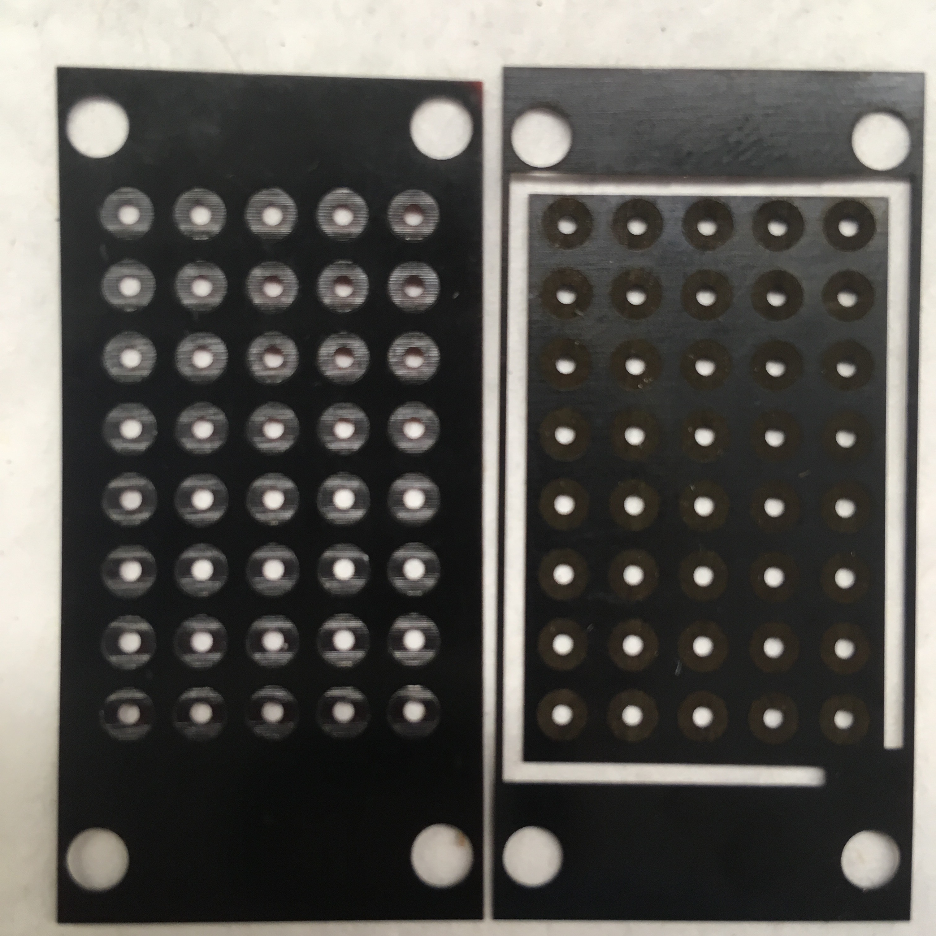
Left: Orignal etch; Right: New etch
Left: Design #2; Right: Design #1
Today my main priority was to work on the new Kapton molds. Even though we are probably going to change some dimensions (like the width of the pillars and perhaps the diameter of the yolks) I wanted to experiment first with the border walls we wanted to add for structural integrity.
Initially, I came up with two designs. Design #1 forms a near complete rectangular path around the border of the Kapton. After cutting this with the UV laser cutter, I realized that there was not enough material to keep the Kapton because one side was almost completely cut away. This should have been obvious I guess, but I didn�t think about it when I was looking at the CAD. Design #2 was slightly more reinforced with one side an L and the other segmented away from the bottom cutout. I was not entirely convinced that this mold was as robust as it could be, and I worry about its performance over time.
Etching with the UV laser cuter was more difficult than I expected. I used Stephanie�s settings for the original mold, except only later did I realize that it appeared that the etchings were 1mil or 2mil shallower than the original. This will be something I will take more time to investigate when I have an improved design. From the photo, it is clear that the etching on the left have a more finished, clean appearance in comparison to the rust-colored etchings on the right.
During this molding process, I experimented with using tape to cover the connection flap on the fabric and I also found short 0.125� pins that won�t interfere with the weights during the curing process. With a more even distribution of weight, I�m hoping that molds have a more even silicone layer.
Week 5
July 19
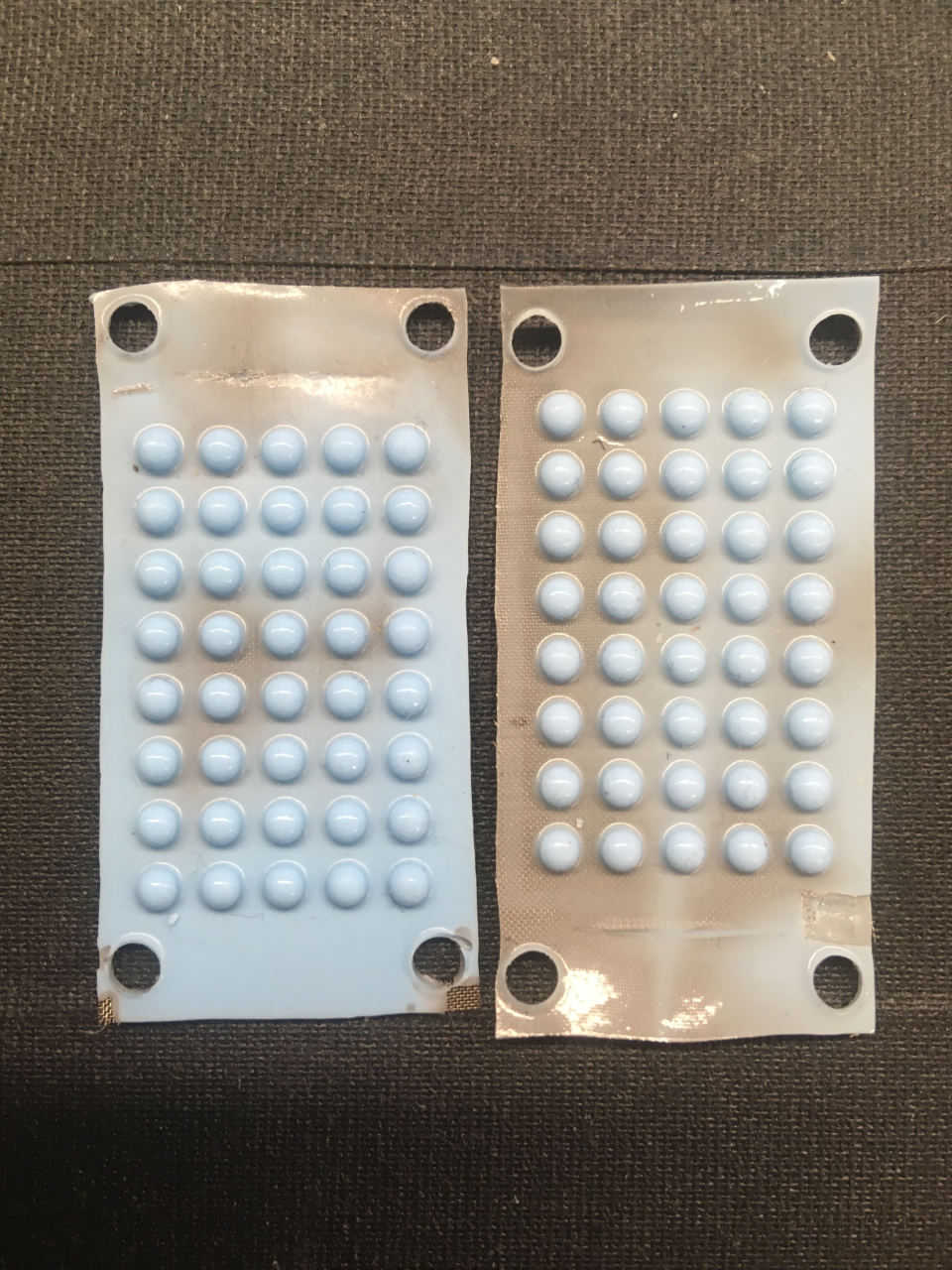
Left: Round-top geometry; Right: Pencil-top geometry
Today is lab bbq! But also the new molds have completely cured. Surprisingly, even without mold release, the molds turned out very promising. There are no visible bubbles on the top or bottom of the molds and each nib appears to be uniform. There is a significant layer of silicone that covers the entirety of the fabric, which will make adhering it to the PCB and to the ground connection difficult, however I find the results satisfactory. Some of the spilled silicone was removed easily with a blade, so I think that if I cover the connection flap with a little bit of kapton tape next time, and improve the alignment I think that the Objet 3D-printed molds will be sufficient to achieve the rounded geometry that we want. Hojung says that the order of PCBs should come in next Tuesday, so by then I hope to also have the new Kapton layer design, the 1/8" 3D-print molds and more fabric layers so that I can start making functioning samples.
During the bbq, Mark mentioned that this type silicone tends to do very well in molds and is not as finicky as other silicons like the Dragonskin. However, as Tap Blue tends to be less durable, it may not work for everything. Either way, I'm pleased that the molds turned out well enough to produce what I think will be a testable model. I spent some time afterwards to update the presentation slides for the lab meeting today. I am also revisiting the Kapton layer design. Hopefully I can finish it now and be able to cut it and some new fabrics on Monday so that I can be prepared for the PCBs on Tuesday.
July 18
Sam brought the new printed molds and they look really good! Something that I didn't think about was that it was really difficult to tell the difference between the pencil-top mold and the round-top mold due to the coloring and texture of the material. Since I wanted to cast both I figured I would be able to tell the difference afterwards, but thankfully Hojung suggested to put them under the microscope and I was just barely able to tell. I labeled them with a sharpie, but I decided for a reprint I should fillet the sides of the rounded molds and leave the pencil top molds with sharp edges. The 1/8" molds and the 1/16" molds will be different thicknesses and easier to distinguish.
After
Before
I had two post-cut fabrics left so I could only make two more molds. I decided to test my skills and try to do both at the same time. It ended up going well at first, but I made some easy mistakes I will record here in order to improve for the next round. (For example I forgot mold release, which was not needed for the acrylic molds but that Hojung suggested for these molds) Something a little odd about this process is that the new molds cannot be poured from the top. Both the bottom and top have to poured separately and then sandwiched together. This means that there's a lot of excess silicone that spills out from the side. I think for the next round of molding, I will "squeegee" the 3d-print mold with a blade and apply a generous amount to the fabric side so that when the parts are sandwiched there will be less excess silicone. I also realized that the 3d-printed alignment holes are slightly undersized, so this makes alignment difficult. I suspect that I will have an uneven layer of silicone. It makes sense that even though I used to same diameter as the laser cut molds, because the plastic isn't melting from a laser, the fit would be more snug with the 3d-mold.
July 17
Roundness is barely detectable
Good news and bad news with the mold this morning. In general, I would say this is the best mold I�ve made this summer. The bottom and top side of the mold filled completely. There are no visible bubbles on the columns and silicone appears to have permeated completely though the conductive fabric. It appears that flipping the mold upside down during the curing process helped fill the columns completely. We did not achieve the domed/rounded end that we were looking for. Hojung has made an interesting suggestion that I could use a toothpick or a pipet to add a little blob/shape to end of each column to help along the forming of the meniscus.
It is important to mention that I used the 1/16� top acrylic instead of the 1/8� but I am assuming to find similar success in this flipping method for the longer columns. Also important to note that I think I also improved the timing of the degassing process. During the first spread over the fabric layer, I degassed the mixed silicone and the mold for about 5 minutes (or until it appeared no more large bubbles were forming). After the spreading the top layer, I degassed for the full 10 minutes and then spread a final layer that was not degassed and allowed to cure.
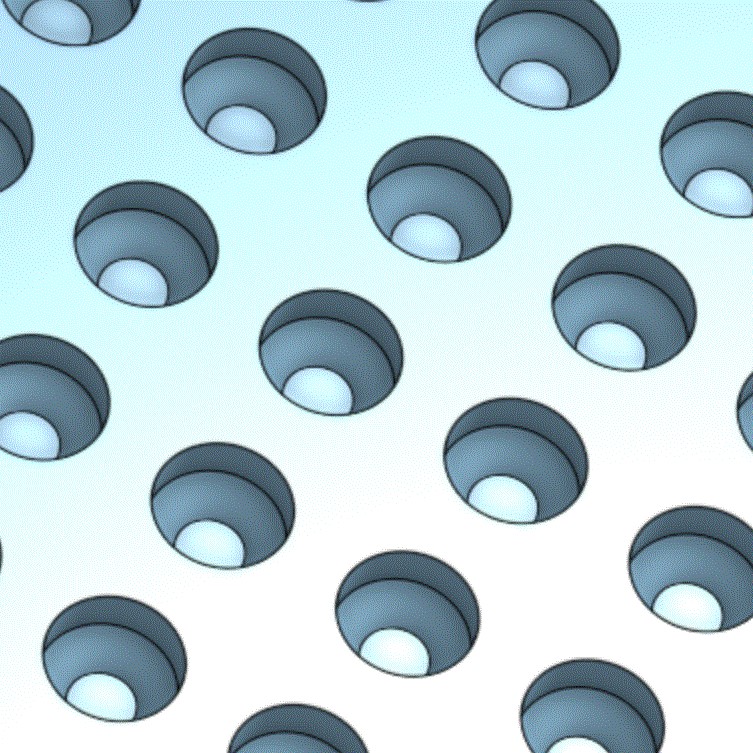
Conical design, aka �Pencil-tip�
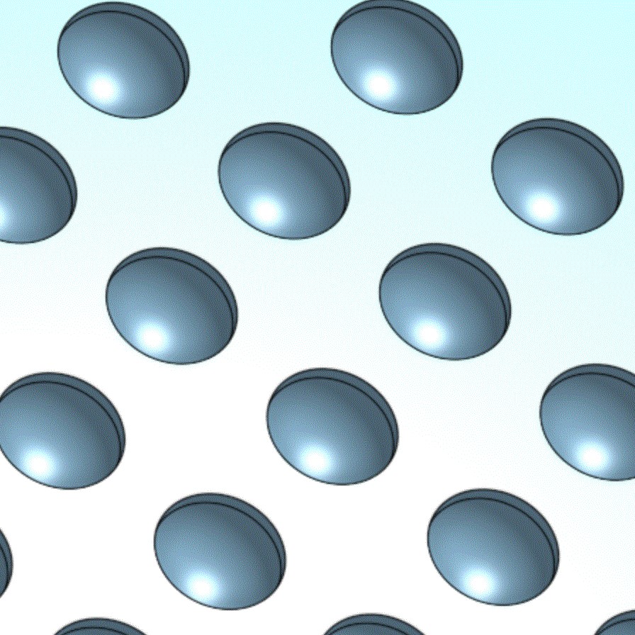
Spherical design, aka �Round-tip�
Moving forward, I finished up the CAD for the new sensor molds so that they could be printed with the Objet. We want to try two designs. A true �round-tip� design with a hemispherical mold pattern. The second design is a conical �pencil-tip� design. Some parameters are experimental � for example, the end of the pencil-tip is 0.05� or half the diameter of the column itself. We suspect that a smaller diameter tip might increase sensitivity. I made two versions of each mold for 1/8� and 1/16� columns. For the pencil-tip 1/8� mold, instead of adding more material to the cylindrical base, I made the cone portion of the mold steeper because that seemed like a more interesting parameter to mess with.
July 16
I spent this morning making new acrylic layers for the sensor mold. Hojung and Tae have performed a different type of test on the sensor. Instead of moving the test mount, they attached a piece of acrylic to the muscle force tester and sandwiched the acrylic between the sensor and the testing mount. We learned that while our sensor detects shear force very well, it does not detect slip vibration in this set up. Some of the literature I've been reading has confirmed that flat-top nibs have difficulty detecting slip vibration on smooth surfaces, but round-top nibs can. We have yet another reason to pursue a new sensor design with round nibs.
I spent the remainder of my day decided on how to best achieve the round-top nibs without completely changing the fabrication process. So far, we have isolated three options. First, 3D-print a mold using the Objet printer (which has a very fine resolution). I have already started to make the CAD for this mold. Second, as was done with a previous sensor design, using a ball-end tool and the CNC to cut a mold. This would take more time, obviously, but sounds like a sure bet. Third, as suggested by Alex during last weeks sensor meeting, we could simply flip the mold upside down while it cures so that a domed meniscus forms. Given that I already had a primed fabric, I decided to try out the third option today.
I spent the rest of the day designing a new bottom acrylic layer such that the menisci could form but weights could also still be applied on the top. I cut the new layer using the laser cutter at Room36 and spent the remainder of my afternoon preparing the mold. Tomorrow we shall see if I was successful. Some troubleshooting is needed: normally we apply an excess amount of silicone on the top layer and Dr.Blade the excess AFTER the silicone has cured. This time I had to Dr.Blade immediately so that when it does cure, the menisci aren't tampered with during the removal of the molds. We shall see if the columns fill. I chose to make them 1/16" instead of 1/8" in case that helps allow them to fill completely.
July 15
This morning, I read some more papers about sensors with �nibs� and I caught up on the force simulations Hojung had been running in order to optimize the sensor nib geometry. He discussed the parameters he was working with (yolk diameter, yolk height, nib height, nib diameter) and what he wants to simulate further. We ended up talking about the possible benefits of moving forward with round-top nibs. Before the SURI meeting, I also made a quick trip to the PRL to laser cut the new alignment plate that I designed last week for the test set-up.
For most of today, Hojung and I ran the preliminary tests on the newest sensor (sensor #2) with the longer 1/8� nibs. First, we tested for slip vibrations along the length of the sensor using the new, full end effector. After finding the initial position, the parameters we wanted to change and investigate were as follows: the applied normal force (z-displacement) and the speed the applied shear force (either changing the time period or the x/y-displacement.) Interesting to note: because of the placement on the bolts on the F/T Sensor, the adjustment of the y-displacement (along the width of the sensor) is extremely limited.
We were able to make some interesting initial observations. First, we tested slip along the length of the sensor. Increasing the z-displacement beyond 1mm would apply too much pressure to the nibs and does not allow a detectable slip vibration. Increasing the speed of the shear force seemed to increase the slip vibration signal---but might also increase the noise signal (more testing for this is needed.) When we switched to test along the width of the sensor, we were unable to produce a good slip vibration. We also noticed that the �signal pairs� were far less symmetrical, suggesting a potential misalignment in either the yolk part of the columns or perhaps a non-uniform tension within the fabric. In general, we saw a deteriorate in the quality of our signals over time, along both the width and length of the sensor. Some unconfirmed theories about the source of this deterioration is that the yolks are being peeled up from the PCB board. Although we cannot be certain about this, it does seem that making more experimentally improved sensors will be helpful.
As we are still waiting for the PCB order to arrive, we have some time before we can make new designs, but I will be getting started on making two updates � first, adding a wall to border the PCB and the fabric to improve the integrity of the silicone adhesion; and second, making a new top mold such that the nibs will have a rounded profile instead of a rectangular one. For the latter, I will attempt to make a 3D-printed mold for the Objet printer. If the resolution is not fine enough, Tae mentioned we may need to make a special tool and use the CNC (but we will attempt to avoid this option.)
Week 4
July 11
Designed to cover all sensor papillae
This morning I collected my finished print and caught up on my blog. Some interesting things to note: the fit of this end effector piece is much looser than the others. I did expect some difference because it is no longer the exact same material/print as the mount, however thankfully my bolt/nut tightening system secures the end piece enough such that I don't think it will effect it's ability to produce accurate test results. I suspect that reason why the fit is different is because the BDML ulitmaker had AA0.25 print core with generic red PLA as opposed to the AA0.4 print core with tough white PLA that I used for the other parts. I also positioned the piece standing up vertically to enable the print without undercuts/overhangs because this printer did not have PVA for supports.
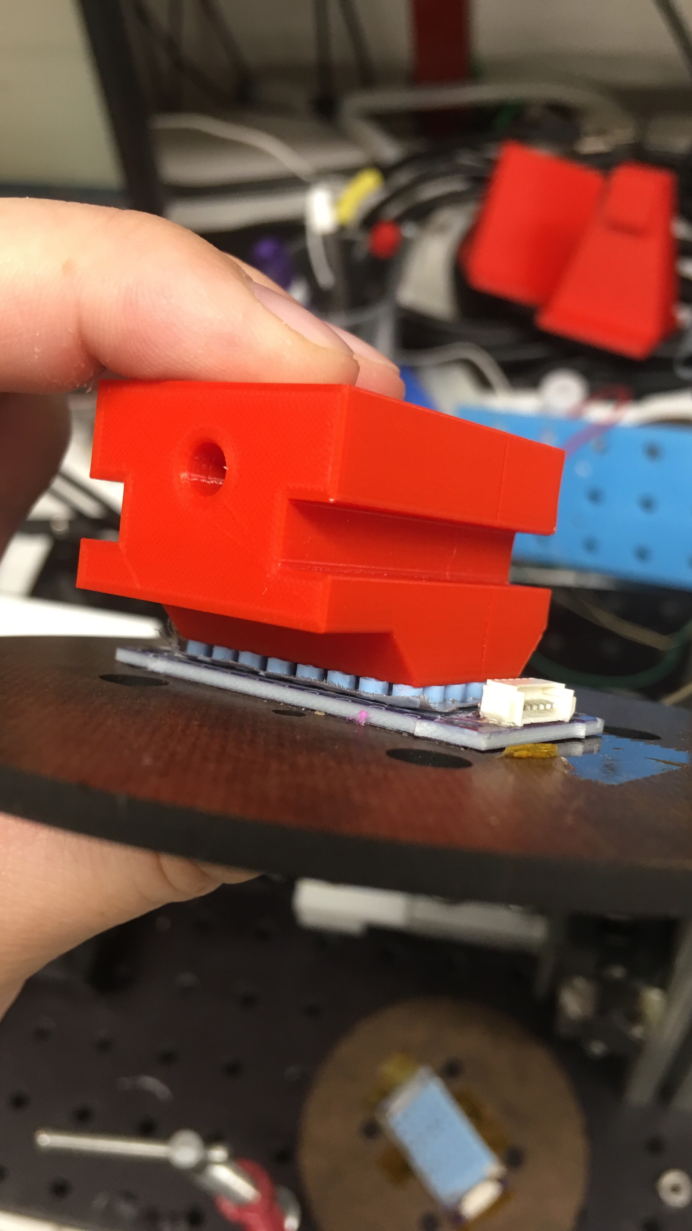
My newest project is to improve the mechanical design of the sensor itself. Right now, the edges of the fabric peel up from the board, and we are concerned that with significant shear stress, the sensor will fail. Tae's suggest was to redesign the Kapton bottom layer to include cutouts for a 1mm high wall to border the edges of the sensor. This wall would adhere to the PCB during the spin layer assembly process. I also have a smaller project of re-designing the Duron plate that we fix the sensors on because right now we are using old plates from an old design. I will also make the plates smaller in diameter to insure that the bolts on the testing mount clear.
I walked Hojung through the Zeber software and he walked me through the tuning process for the sensor again. Stimulating one sensor was enough to produce a good signal, but stimulating multiple sensors produced a far better signal. We will test to see what is the number of columns for a best signal. Hojung also tested the force sensitivity of the sensor by placing a 10 gram and a 2 gram weight on the sensor. It detected the 10 gram weight, but not the 2 gram. He says that for our purposes, that is, picking up dishes and holding items, the 10 gram weight sensitivity was more than satisfactory. 2 gram sensitivity would be more akin to holding a feather.
A random observation is that the columns with base bubbles (picture can be seen at the bottom of my July 9th update) are noticeably softer and compress differently than the others. Tae suggest that when we apply the final layer of silicone during the fabrication process, we should not degas the silicone.
July 10
Please excuse the sub-par soldering
Having finished curing, the sensor was ready in the morning for the final assembly. We used the silver epoxy to adhere the connector flap of the fabric to the ground of the PCB. This needs 4 hours to dry, or 15 minutes in 30 degrees Celsius. We chose the latter and used the toaster oven. Once it was done drying, I soldered the Molex connection to the PCB. Note here: I mistakenly grabbed a Molex that would connect from top to bottom, but we want the one that connects from the side so as to not interfere with the test set-up. Luckily, I realized this before soldering it into place. I had some difficult getting the solder to "stick" to the PCB. This has never happened to me before, but after cleaning the PCB copper plates with very little IPA and then turning up the heat of the soldering iron, I was able to get good connections. They look awful, but I made sure to test them with the multimeter.
Next, I met briefly with Tae and Hojung and we talked about our plans for the next couple weeks as well as the test set-up. Hojung is using a force analysis software to determine if the geometry that was arbitrarily chosen for the sensors (the column geometry of the individual papillae and also the number of rows) can be optimized. Tae is working on the new PCB design. In the simplest of descriptions, right now each "hair" on the board is connected to each other in such a way that the signal generated from the stimulating one column is essentially the same when all the columns are generated (sensitivity does change slightly.) The new concept would be to group the hairs in sets that react differently to specific stimulation. One benefit of this method is that we can "turn off" the papillae that are not being stimulated and improve the signal being generated from the papillae that are being stimulated.
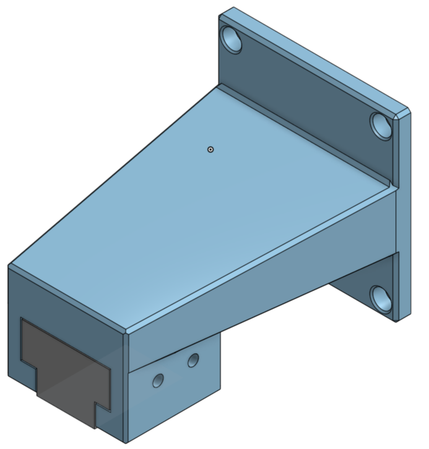
Tae also said that we would need a test set-up that could apply a force to all of the papillae at once. So, I designed an end effector that could do so. This was one of the reasons why I thought my design for the testing mount would be useful. If I had done the print at the PRL, this would have only taken an hour to print and we would be ready to go. Unfortunately, the Ultimaker's were all booked by high school students so I used the lab printer which as a smaller print core and would take the rest of the working day to finish. Either way, this was still more efficient than having to print an entirely new testing mount.
At the end of the day, we had our first tactile sensor meeting of the summer. Mark steered us away from calling the columns "hairs" and instead leaned more towards calling them "papillae" --- like taste buds. It is also possible that we will want rounded tops to our "papillae" and so we have another future task of figuring out how to make mold to achieve that geometry.
July 9
Top: Ho Jung's (brick weight), Bottom: Mine (300 g)
Top: 1/16" columns, Bottom: 1/8" columns)
This morning when I checked on the finished molds, I realized that the columns seemed significantly taller than the columns of the sensors I did with Stephanie. I realized that in the box of molding materials, there are two top acrylic plates of different thickness - 1/16" and 1/8". I was quite frustrated that I had not thought to check this.
Additionally, my mold did not fill completely because of some significant bubbling. Ho Jung's mold appeared to be better, and I believe this was because he used a heavier weight. However, upon looking closer, there were some bubbles at the base of some of his columns. That being said, the columns are taller. We decided to go through the rest of the process with Ho Jung's mold just to test the difference in sensitivity between the 1/16" columns and the 1/8" columns. Tae worries that the taller columns will have more moment force and interfere, and so if the shorter columns are indeed more sensitive as he hypothesizes, we are looking into finding an even thinner acrylic to make even shorter "hairs." However, with preliminary searches (TAP, Amazon, McMaster) 1/32" or 1mm acrylic does not seem to exist (?)
bubble at base of the left column
I spent the rest of the day finishing up Ho Jung's mold. I was a little hesitant to use the wafer spinner at 5000 rpm because last time the acrylic plate flung off. However, I took the time to find the center of the acrylic plate and had no difficulties. With the silicone curing until tomorrow, I took some time to type up the whole procedure process - crediting most of it to Stephanie's process list but also adding a few of my own notes to remember for future molding. For example, using excess primer on the fabric causes it to curl and unusable for molding. Also random note: Everytime I've been saying Mylar in this blog, I should have been saying Kapton. Finally, I spent some time reading more papers (it's slow going, but I think will be useful.)
July 8
Note the pancake shapes vs. the fried egg shapes
Today Ho Jung and I went through the first stage for molding the sensors. My mold from yesterday was *just okay*. A positive result from this mold was that there were no visible holes from bubbles on the bottom side of the conductive fabric. This means with the new step of applying the silicone while the fabric and bottom acrylic layer are already aligned successfully allows the silicone to permeate completely through. A negative result from this mold was that when I applied the double-sided tape, I placed the strip down the center of the mylar layer. This meant that some of the holes were covered from the tape and some were not. The holes that were covered molded perfectly but the holes on the outer edge experienced a �spilling effect.� There were also substantial hole bubbles on the top surface of the columns. With Ho Jung's help, I used the microscope to take some close-ups of the bubbles. The microscope was not a high enough resolution to show the micro-bubbles, but I was a little curious to see how far the visible holes went and also just wanted some cool photos for the blog.
Cross section of same column, note the outline of the bubbles
Close up one of the silicone columns with visible bubbles
For the second round of molding with Ho Jung, we made some adjustments to the fabrication process. First, we covered the whole back of the mylar with double sided tape. Hopefully this eliminates the �spilling effect.� Also, when vacuuming, Ho Jung explained to me the concept of �micro-bubbles�, or bubbles that cannot be seen by human eye, that can really affect silicone sensors particularly when detecting vibrations. As such, we increased the vacuum time to 10 minutes. However, we noticed that with the limited pot time of the silicone, once we vacuum the first layer, filling up the columns for the second layer is difficult. We are curious if adding more weight will help mediate this, so we used the heavy brick weights on Ho Jung�s mold, and I used the same 300g weight on mine.
An idea I thought of was that maybe we can mix a small amount of silicone for the first layer and then about 7-8 minutes into its vacuum time, we can mix another small amount of silicone so for the second layer so it is less tacky and fills the columns more evenly. This would be an added step to the fabrication process but might be worth to eliminate microbubbles but also fill the columns.
Also, Mark mentioned the possibility of producing a paper for these tactile sensors. Tae spent a little time explaining what that would like and the deadline for a possible conference to submit the paper to. This seems like a really exciting opportunity!
Week 3
July 5
I had a productive Friday! Today Tae returned to the lab and he worked with me all morning just to catch me up on all the sensor stuff. He explained the experiments I would be running on the sensors in greater detail and slowly walked me through how to use the console/different pins and how to tune the signal from the sensor to acquire usable data. In turn, I did my best to answer his questions about the sensor mold process form what I remembered from Stephanie. Also, turns out the crimping that I had done last week was completely wrong, and so Tae showed me how to correctly crimp - which was still difficult and took a long time, but I think I finally got it.
Back when Stephanie and I made our sensors, recall that mine was made with thicker conductive fabric while Stephanie's was made with thinner. With the thinner fabric, the silicone was able to permeate through the mesh and adhere with PCB board. However, the thinner fabric tore easily and shredded along the alignment holes. In contrast, the thicker fabric was easier to work with and align, but did not allow the silicone to fully permeate and therefore made an unsatisfactory connection with the PCB. As a solution, I went back on the CAD file for the fabric and added more material to the sides of the fabric so that the alignment holes would be more reinforced. After lunch, Tae accompanied me to the CHARM lab and I cut the pieces on the UV laser (yay! learning a new tool!)
Then I spent the afternoon doing the first stage of the silicone mold. There's a high probability I forgot a step, so I might be redoing the mold on Monday, but here's a step-by-step of what I did so I can remember what I did wrong or right depending on what it looks like after it cures. I suspect I forgot something important, like taping down the edges of the fabric (?). I also forgot to use mold release ): Toothpicks also might have been easier to work with than the popsicle sticks.
Used 300g of weight, may want more
1) Set up mold
        - Bottom to top: Thick acrylic plate, double sided tape, mylar sheet, fabric, dowels, thin acrylic plate
        - Remember to orient the sheets correctly (align the sides based on the PCB orientation)
        - Four dowel pins for initial alignment, but two for actual mold because mylar will wrinkle
2) Make silicone
        - 10:1 (Tap Blue), zero scale
        - mix, timer for pottime
        - vacuum to remove air bubbles
3) Spread evenly over fabric layer first
- vacuum
4) Place thin acrylic plate
- spread generously, vacuum
5) Scrape excess
- Doctor blade
6) Place spare acrylic over, apply weights
- Let sit for 10 hours (?)
July 3
I spent sometime in the morning to edit the other two t-slot ends that I wanted to print. I wanted this to be exact because it was important that the each end piece did not interfere with parts of the sensor that aren't being tested (ie. for the 3x3 array end effector, I wanted to make sure it would not partially cover any other silicone columns.) Additionally, even though I added a fillet to the first point end effector, I did not feet that it was as robust as it should be, so I added substantial chamfers to the other two.
Right to left: row detection, point detection, 3x3 array detection
I went back to RM36 to print out the other two testing ends for the mount. 3D-printing went a lot faster this time around, which felt good because I think the tutorial yesterday paid off. While I waited on the print, I read up on the UV laser because Stephanie wants me to make another sensor mold down the line and I also caught on some of the literature she sent me for tactile sensing and slip detection (I have a lot still to read.)
For some reason the fits of the second and third end effectors were far more snug than the first one, so I spent some time filing down the edges and wet-sanding for a more manageable fit. But this project is done! I"m pretty satisfied by how easy it is to switch between end effectors but still have a stable, reliable mount for the force detection set up.
July 2
Note the substantial supports and adhesion material
I collected my pieces from RM 36 in the morning. They turned out surprisingly well but I was concerned about removing the "natural PVA" because I couldn't really see if the parts fit properly until I did. I ended up leaving the parts in some water and putting it out on the sun for an hour or so. Afterwards, I was able to pretty easily remove the PVA with pliers. The print wasn't perfect, but I spent a little time post-machining in the hope that I would not need to do another 7 hour print for the mount. For example, the t-slot actually did fit pretty well after some rough sanding. Additionally, the holes for the bolt that connects the mount to the Zeber console was slightly undersized, but I was afraid that if I used the end mill, it would break the thin walls. Fortunately, the bolts do work, it's just a very snug fit.
I made the silicone sensor, the Molex wire, and the testing mount in this photo!
I made some notes of notable changes that I would want to make if I had to make a new print for the mount, but that aren't necessary at the moment. In general, I'm really happy with my design! The end piece removes easily from the mount and installation/tool placement is really simple and easy. I installed it on to the Zeber console to make sure the dimensions were correct. I was slightly concerned about this because I used my own measurements from the former mount without any reference to its CAD file, but it seemed to be pretty accurate.
July 1
Today was a CAD day. After looking at my design from last week, I really felt like it could be better. Because the Ultimaker in the lab was being used anyways, I spent sometime thinking about what I could to make it better. My biggest concern was that the t-slot would not be a good enough fit to perform well under the test conditions. We want to minimalism vibrations since that sliding vibrations are the phenomenon we are trying to understand. Another concern was that the testing set-up would need be to lowered because of the extra material I added to the mount. I felt like I could do better.
"Old" design, more parts/material, t-slot inserts from front
After the SURI lunch meeting, I ended up spending much of the day at Room 36. It took me a moment to get approved, but I eventually got a pass. The shop CA there helped me approach my design in a different way, and we talked about constraints and degrees of freedom. After talking to him, I ended up coming up with a different, more material efficient design with a lower part count. The idea with the new design is to use a bolt to pull in the t-slot to the side of the mount. The big idea here was using pre-load (with the bolt acting as a pre-loaded spring) instead of forcing the sides of the mount to deform and "clamp" on to the end piece. The t-slot end piece also installs from the side for easier tool placement which was something I wanted to prioritize since test set-up would need to be moved around.
"Updated" design, less parts/material, t-slot inserts from side
I also got a lengthy but basic tutorial on 3D-printing from the shop CA. I also downloaded CURA so I could go through the terminology (fill, line height, build plate adhesion, etc.) We talked about the different printers, support materials, managing undercuts, and in general how to use the Ultimaker. I ended up using tough PLA for the part and a natural water soluble material (that I forgot the name of) for the supports. I only printed one of the end-pieces because I predict I will need to make edits to the parts end/or use a different type of printer.
Week 2
June 28
Today was lab clean-up. Mela and I must have sorted a 100 different types of resistors and miscellaneous electronic parts. This morning we also had a full lab meeting with Mark over Skype and he talked about the different research and projects that he saw in Italy like the shower helper robot, the octopus robot and (my personal favorite) the grass cutting robot.
End effector for a single silicone "hair"
End effector for a 3x3 array of silicone "hair"
End effector for a row of silicone "hair"
Most of the day was spent cleaning, but I did have time to start making edits on my new parts. It has been a little difficult getting used to OnShape, particularly the part studio feature. After Stephanie and I discussed some edits to my part, she gave me a brief tutorial about referencing parts and the boolean/union feature. I ended up starting over with my end effectors to accommodate my edits on the mount base. For example, for the t-slot parts to slide effectively, Stephanie suggested we offset the two parts by 0.015". Applying the offset feature on the boolean tool made this step easy. Additionally, some of the walls were 1/4 cm thick, which Stephanie was worried would be too thin and fail during testing. I changed the design so that no wall was thinner than 1/2 cm thick.
I was a little disappointed because I wanted to finish in time to print at RM36 but it was alot harder to make the edits as fast as I wanted using OnShape, which I'm still getting used to. Another SURI needed to use the 3D printer anyway so I decided to simply print next week.
June 27
Today, the morning passed by quickly (in a good way.) I accompanied Stephanie and Andrew to the CHARM lab and I observed as he used the UV laser cutter. The piece being cut was small copper conductor wiring adhered to a sheet of glass using a thin layer of dragon skin silicone. The copper was cut in a serpentine shape to accommodate the bending and rotation of the robot hand, since copper is not elastic. I learned about the different settings of the cutter and how to layer sketches so you can etch and cut at the same time.
Close up of the silicone mold
The molds from yesterday were now ready, so Stephanie and I cut away the excess silicone and soldered the male Molex connector onto the PCB. The connections were very small but doable. Then we used silver epoxy to adhere and make the connection between the PCB and the conductive fabric. For some reason, I got really excited when I heard the short circuit beep from the multimeter when I put one lead on the PCB ground and the other on the conductive fabric. I think it was hard for me to believe that the fabric was conductive until I tested it!
I spent some time redoing some of the crimped wires from yesterday ): I have also started some OnShape - concentrating on Part Studio and Assembly tutorials because that seems to be the feature most relevantly different from SolidWorks.
New mount design
Stephanie gave me a project to work on! The testing set-up for the finger pad sensors currently uses a 3d printed piece to apply the force evenly on the sensor. However, with the new sensor design, Stephanie wants me to redesign the mount piece such that a single pad, a row of pads and an array of pads can all be tested with minimal assembly between set-ups. I came up with t-slot design so that three different end pieces could slide in and out easily between testings and be secured with a pin. I finished the design, but I want another day.
June 26
This morning I spent some time crimping the second half of wires for the Molex connector. I was much better at using the Molex crimping tool today than I was yesterday. After installing them into the female connector, I wrapped the wires in aluminum foil. Stephanie explained that this was a quick and dirty method to limiting noise from interfering with the sensors signals. I thought that was really cool and I wish I had known that for my ME210 robot because we actually had some troubles with interference.
Silicone molds after wafer spin
After this, Stephanie and I went through the next steps for casting the silicone molds. I think today I began to appreciate the methods and intense order of operations that needed to be planned before making actual molds. Waiting for cure times and primer dry times throughout the day really put the process into perspective. With our fully cured molds from yesterday, we made a thin membrane of silicone over the PCB. We lined the electrodes with tape to keep them exposed for soldering and then lined the edges with tape again to act as a shim - preventing the new silicone from covering up the smaller details of yesterday's mold. We primed the PCB with ABT primer first, which took two hours to dry. I mixed the silicone and degassed with the vacuum chamber by myself. Then, Stephanie showed me how to use the wafer spinner. I found the process really interesting and fun to do, even though my acrylic base kept flinging off (We decided to mark the exact center for future iterations.)
With these molds curing until tomorrow, I spent the rest of my day starting and finishing the lengthy Laser Safety Training so that I could work with the UV laser cutter. Late in the evening, I was able to join Stephanie and Hojung on a skype call. This was a long but really neat meeting where Stephanie went in depth about the sensor project. She went over all her past research/experience, the new design, and what to look forward to. I was glad I was at this meeting, because although I have tried to absorb as much as I could about the sensor mold as I was making it, I found a lot of what I had been wondering about the past two days to be cleared up easily during the presentation. It was actually neat to have made the silicone piece prior to the breakdown of the project because I felt like I had a higher-level of understanding and interest.
June 25
Although there wasn't a formal NASA meeting today, Tony let me sit in with him and Rob and he went over the projects he had been working on in the past. I watched the videos of the gripper prototypes catching "spinning objects" last night but it was interesting to hear Tony explain it in person. I found it exciting that the projects were already sent to NASA to be implemented. He also talked the new NASA grant he wanted to secure and the 2-3 ideas he and Rob were researching at the moment. I found the idea of implementing the gecko adhesives on a rover to be really interesting. I like the idea of ideating small projects and pumping out prototypes before settling on a larger project for the grant. He said his research this summer would have soft timelines and that he wants to come up with at least 10 ideas/prototypes and that if I had any ideas, that could be something for me to work on this summer. I find it slightly out of my depth to think about new ways to apply the gecko adhesive in space, but I would be excited to work on something so new if I did.
I spent the rest of my day shadowing Stephanie. She walked me through the silicone mold process. I had never worked with silicons before and it felt good to do some hands-on work. She explained what the process was, how to select different silicons based on their physical properties, and important properties like the mixing ratios of part A and part B, pot time, and cure time. She also explained the functionality of the different layers of the sensor: the acrylic bases, the mylar layer, the silicone columns and the custom PCB. I enjoyed mixing the silicone, making the mold, using the vacuum chamber to remove air pockets, and in general observing the process from start to finish. The process reminded me of sand casting but of course, with silicone and at smaller scale. We also went over the uses of the wafer spinner in applying even layers of silicone. Although I do not think I succeeded in applying enough pressure and eliminating the air pockets in my mold (we each did one, mine with a thicker fabric layer), I am excited to see what it looks like tomorrow. We briefly looked at the OnShape files for her parts. I am thinking about spending some time doing some tutorials because while I feel familiar with SolidWorks, she showed me some features unique to OnShape that seemed extremely useful for things like part editing with references to other parts
I spent the final moments of my day at the lab learning how to crimp wires for the molex that we will need to use for the wiring of the force sensor. I've only observed crimping, so it took a while to get a hang of it particularly with the tiny crimps we were using. I was able to get half of the crimping done but I plan on finishing it tomorrow morning.
Today I also spent some of my morning to start the online safety training (EHS-4200, EHS-1900, EHS-3850) and then finished them during lunch. I think I will also do the laser safety training because the UV laser cutter seems really cool and I want to be able to use it sometime this summer.
June 24
I started SURI later than I would have liked due to other job commitments, which has thrown me off somewhat. However, I am eager to get started and commit my summer towards this opportunity to work in this lab. I am excited to contribute and learn from all the fascinating projects going on at BDML. This morning, I arrived at the lab to sit in on a 8am phone conference with Amar and Capella as they presented their findings with manufacturing an aluminum mold for the gecko adhesive. It was interesting to see the "doubling" phenomena that occurred when cutting the metal. The presentation also covered why they chose Aluminum 1001 for the mold, as opposed to tin (which was too soft) or other metals, as well as why they selected a diamond-coated tool. In ME203, the concept of a tool breaking or wearing down was something mentioned but not really discussed or put into perspective so it was interesting to see tool durability as relevant and important factor being considered in the manufacturing process of the gecko adhesive. Aside from articles, I had little experience with the recent updates on the gecko adhesive, so Amar and Capella shared with me the benefits of having a durable, metal mold to manufacture the adhesive as well as the different types of testing they had been doing to move this project forward.
Later, I met some of the other PHds working in the lab, and got a chance meet with Stephanie (which was great because I knew her from a previous class) and she walked me through the research she was working on. I am not very familiar with sensors, but it was interesting to see the molds she made for the tiny, capacitor sensors as well as the small, coin-sized PCB force sensors that the team had been testing. It was neat to directly see and compare the industry/regular sized force sensor in comparison to the new, coin-sized force sensors. We talked a little bit about the applications of the smaller, thinner sensors.
I also spent some time looking at UR5 programming tutorials. I did not get very far, but Mark mentioned I could be using it for a project, so I wanted to look at it before meeting with Jean-Philippe (who I've been told is a UR5 god). Additionally, the SURI cohort met for lunch today and we heard from two students working in the CHARM lab and the IRIS lab. I found the presentation on "soft" vine robots particularly interesting.
Week 1
June 18
Today is my 21st birthday, so I was unable to be at the lab in person. However, late this morning I skyped in a joint-call with Mark, the other SURIs associated with the lab, and Alex (I believe) to talk about our backgrounds, interests, and the current projects we could possibly work on. Late in spring quarter, Mark gave me the opportunity to jump in a Ocean 1k design meeting, where the project team discussed the hands of the Ocean 1k robot - specifically the transition from three fingers to four fingers as well as the different types of cable/pulley mechanisms that could be used to achieve the desired degrees of freedom. I still think this would be interesting to work on this summer.
category: SummerBlogs