category: Manufacturing
Printed Circuit Boards
Vendor Options:
- Regular PBC Manufacturers:
- advance circuits ($33 dollar 2 layer boards/$66 dollar multilayer boards) - 1 week turnaround - put student in the comment section and you can order 1 instead of 4 boards min: http://www.4pcb.com/33-each-pcbs/
- Sunstone for irregularly shaped boards/fast turnaround (3 days + 2 day shipping) (http://www.sunstone.com/pcb-products/pcb-quickturn/pcb-quickturn-pricing)
- bay area http://bayareacircuits.com/ - quick turn around time (less than a week) and they have a student discount (make sure to say student when ordering, can get 7 or so boards for $120). good website for ordering boards
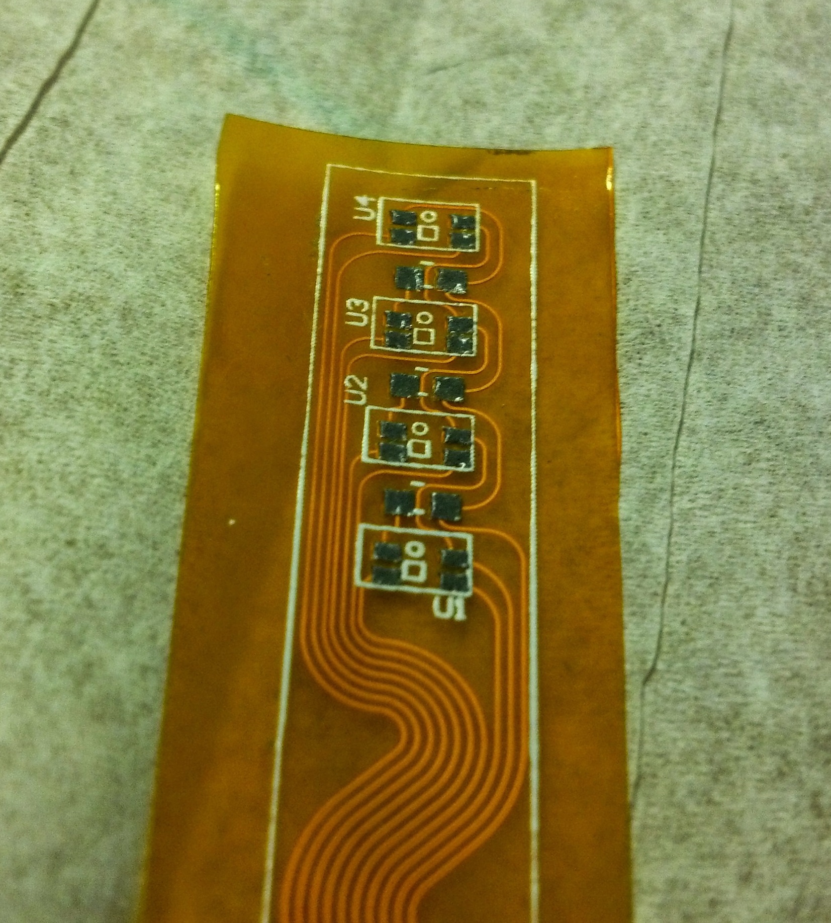
- Flex Circuits:
- Flex Circuit - cheap and extremely fast turn around time (~1 week) - http://imall.iteadstudio.com/open-pcb/pcb-prototyping/2layer-flexible-printed-circuits-fpc-10cm-x-10cm-max.html - they're in ShenZhen, China but speak English perfectly fine. The cool thing about their service is that you can first panelize smaller boards onto the 10x10 cm area and then just cut the flex yourself.
Populating your PCB with components
Luckily, populating rigid and flex circuit boards are almost identical, any details that differ will probably be specific to your board design and materials. These instructions should work for both.
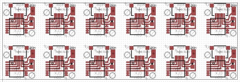
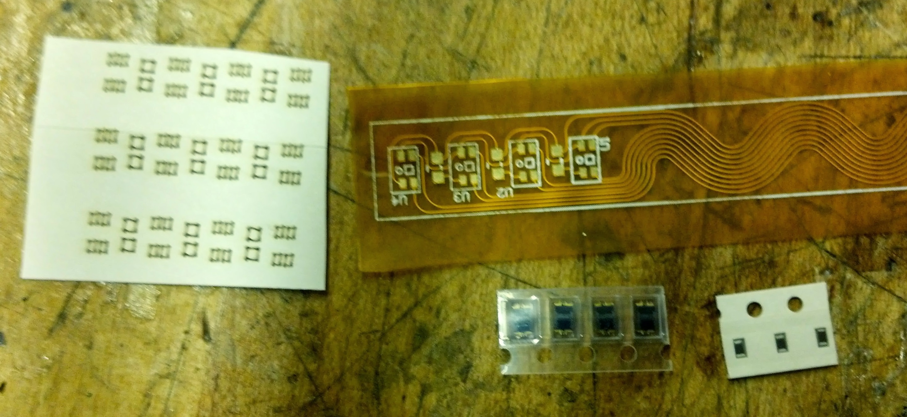
1) It may be much cheaper to pattern your circuit design and order just one board with many. You will then want to machine them apart from one another.
- When cutting fiberglass, use a resperator or dust mask, and safety glasses.
- A bandsaw (TLTL has one) is probably the easiest way to cut them. Leave a little extra material then use the sanding belt to get a nice finish on the edge. Some boards have dowel holes on the sides for lining up the boards during assembly. Do not cut these off prematurely.
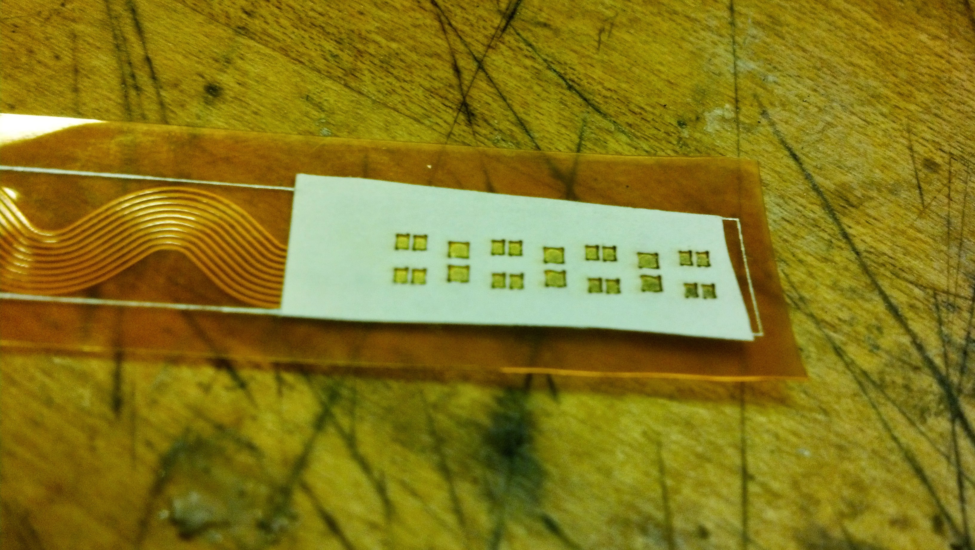
2) Create a stencil for the solder paste.
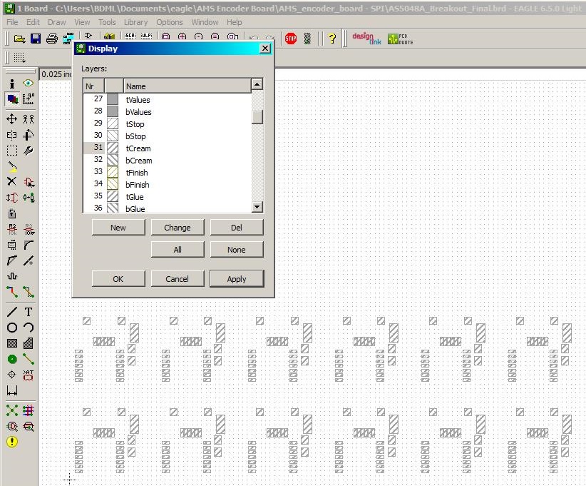
- Open your circuit layout and show only the cream or paste layer you are interested in exposing to solder:
- Altium: tpaste or bpaste
- Eagle: tcream or bcream
- Open your circuit layout and show only the cream or paste layer you are interested in exposing to solder:
- Create a .dxf file of the stencil you will cut on the laser cutter
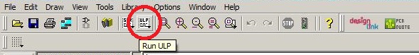
- In Eagle that means running the ULP (User Language Program). There is a button for it on the top quick-menu.
- Create a .dxf file of the stencil you will cut on the laser cutter
- Open dxf.ulp. Make sure you are not exporting the shape filling - you only want the outlines.
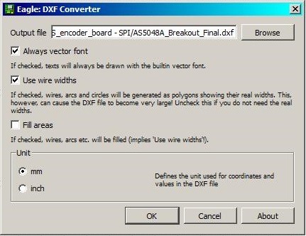
- Verify that your dxf looks right, it should be in the directory of your eagle file.
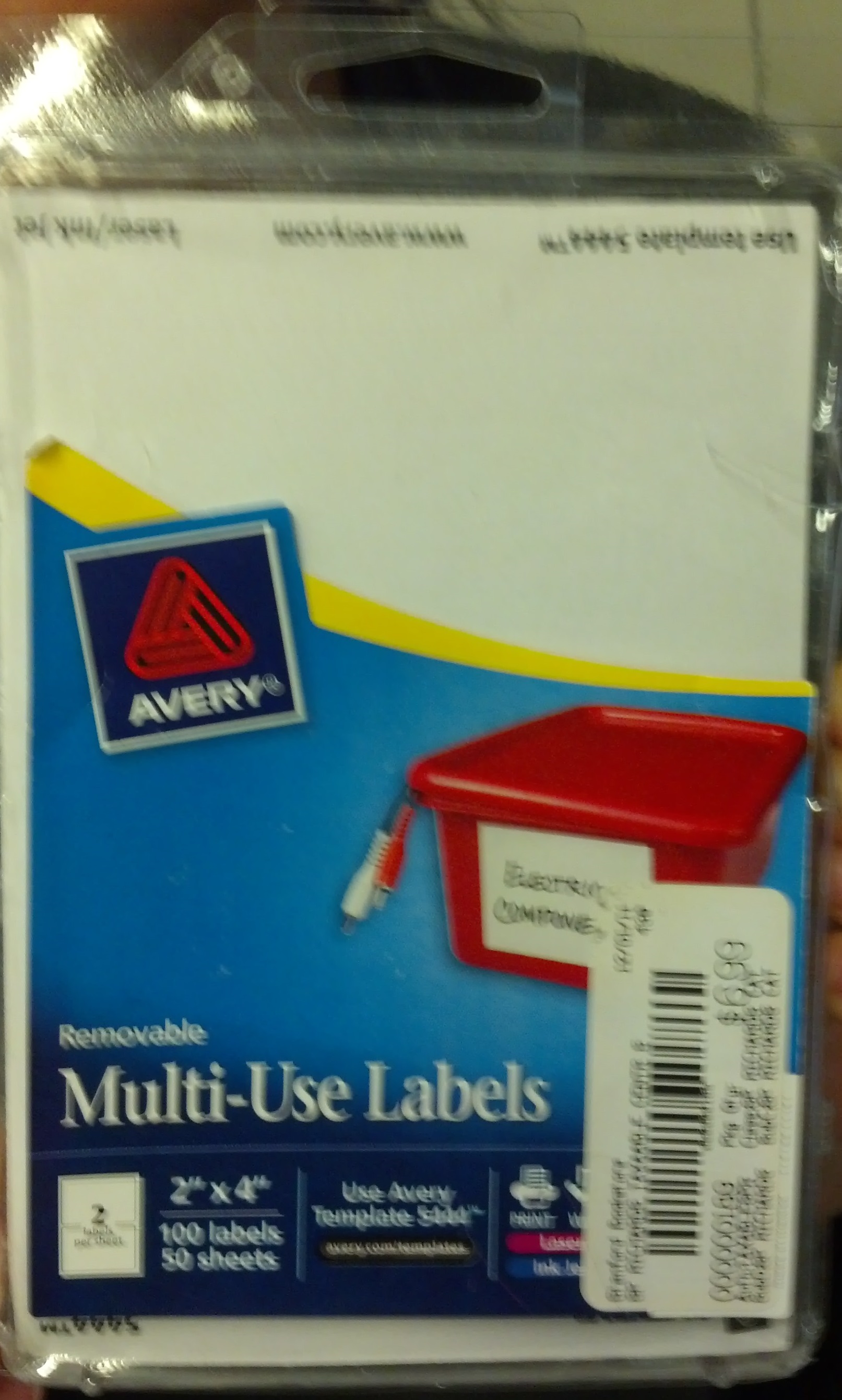
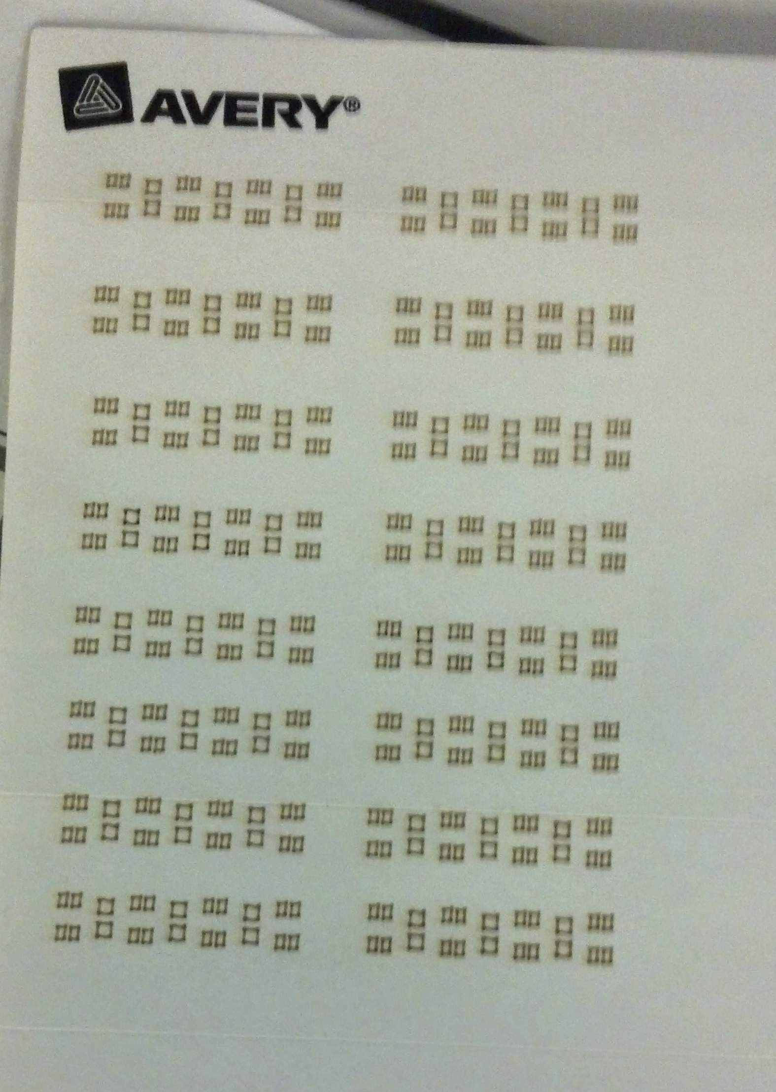
- Laser cut the stencil on stickers:
- 7% power, 90% speed usually works. Do one or two test runs first. Stick with low power high speed. Your cut may not be super accurate when going fast or don't focus properly so be wary of precise stencils with tiny leads.
- With very small close leads, you may have trouble getting a good laser cut. If you look on in the microscope you may see small red filaments at the edges of your stencil, this is a red flag. If they are long enough to connect two leads, then they may short with solder. You can instead cut one slip for all of the leads and cover all of them with solder paste. When it flows, it will go away from the solder mask and with surface tension stick to the legs, removing the shorts. Not intuitive.
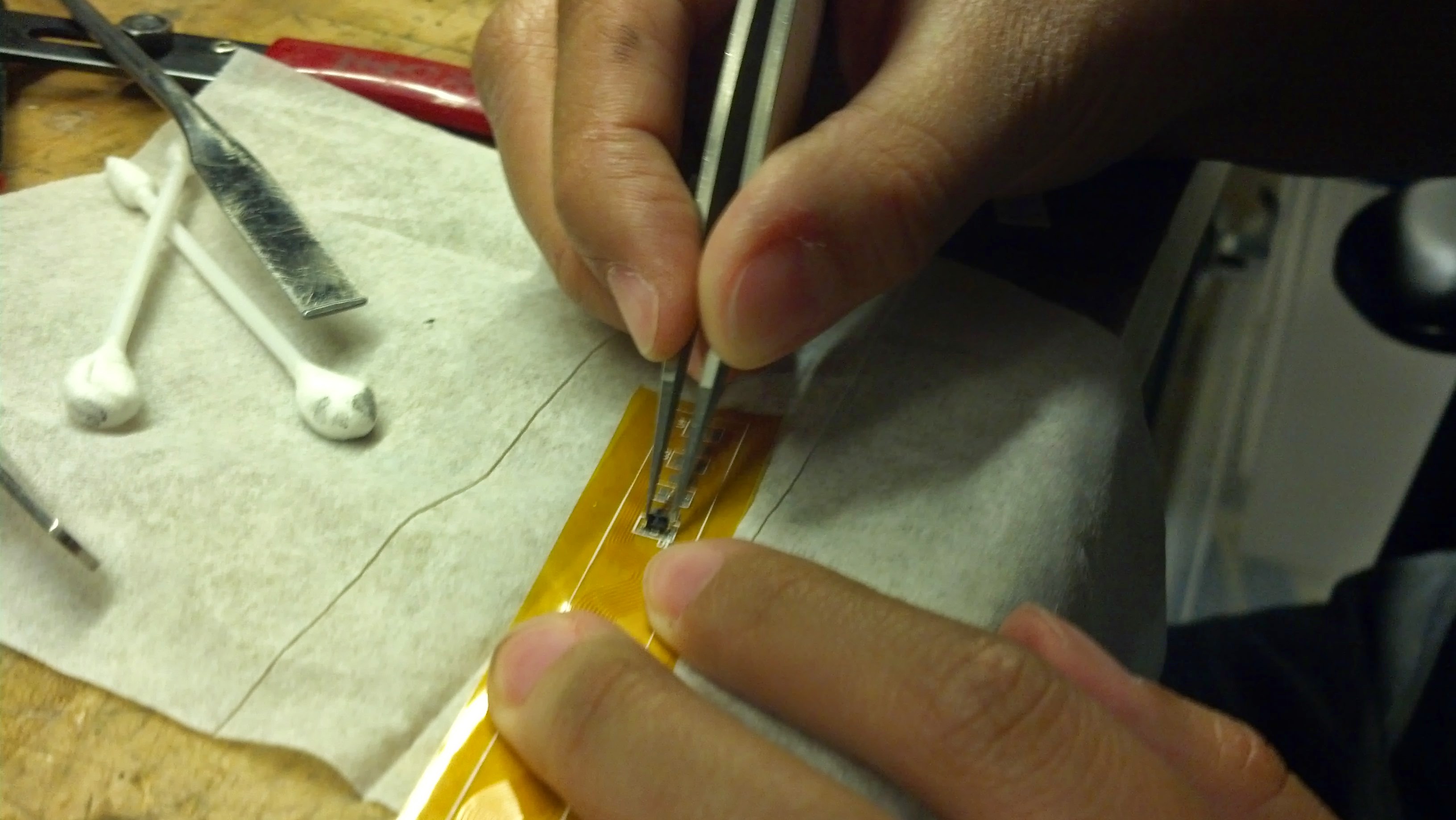
3) Solder the components in place:
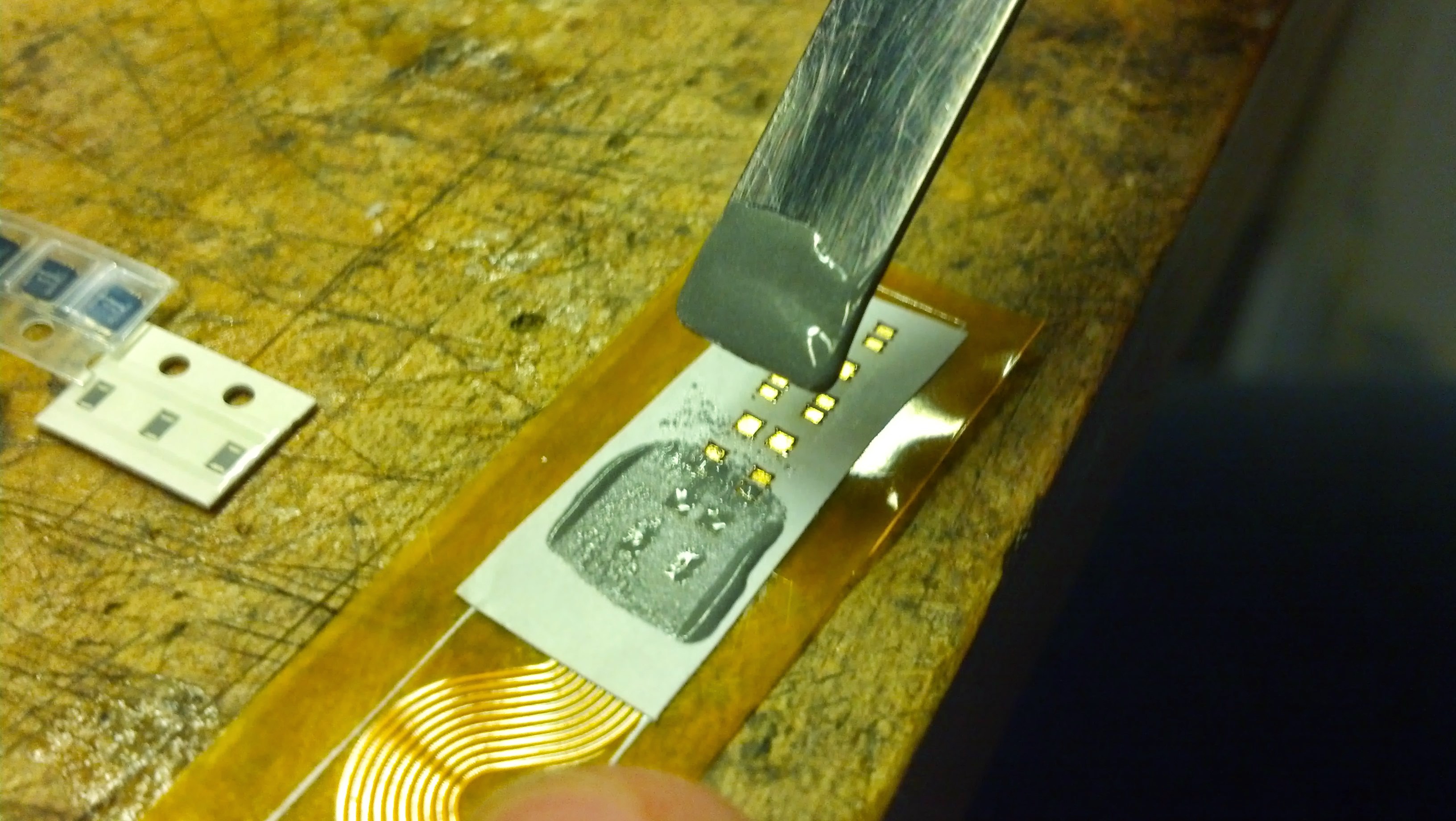
- Apply the stencil to the pcb surface.
- Make sure that all of the desired pads are exposed.
- You can pick off the stencil (tweezers help) and try again if the first application is not right.
- Check under the microscope that the stencil is correctly placed.
- Apply the stencil to the pcb surface.
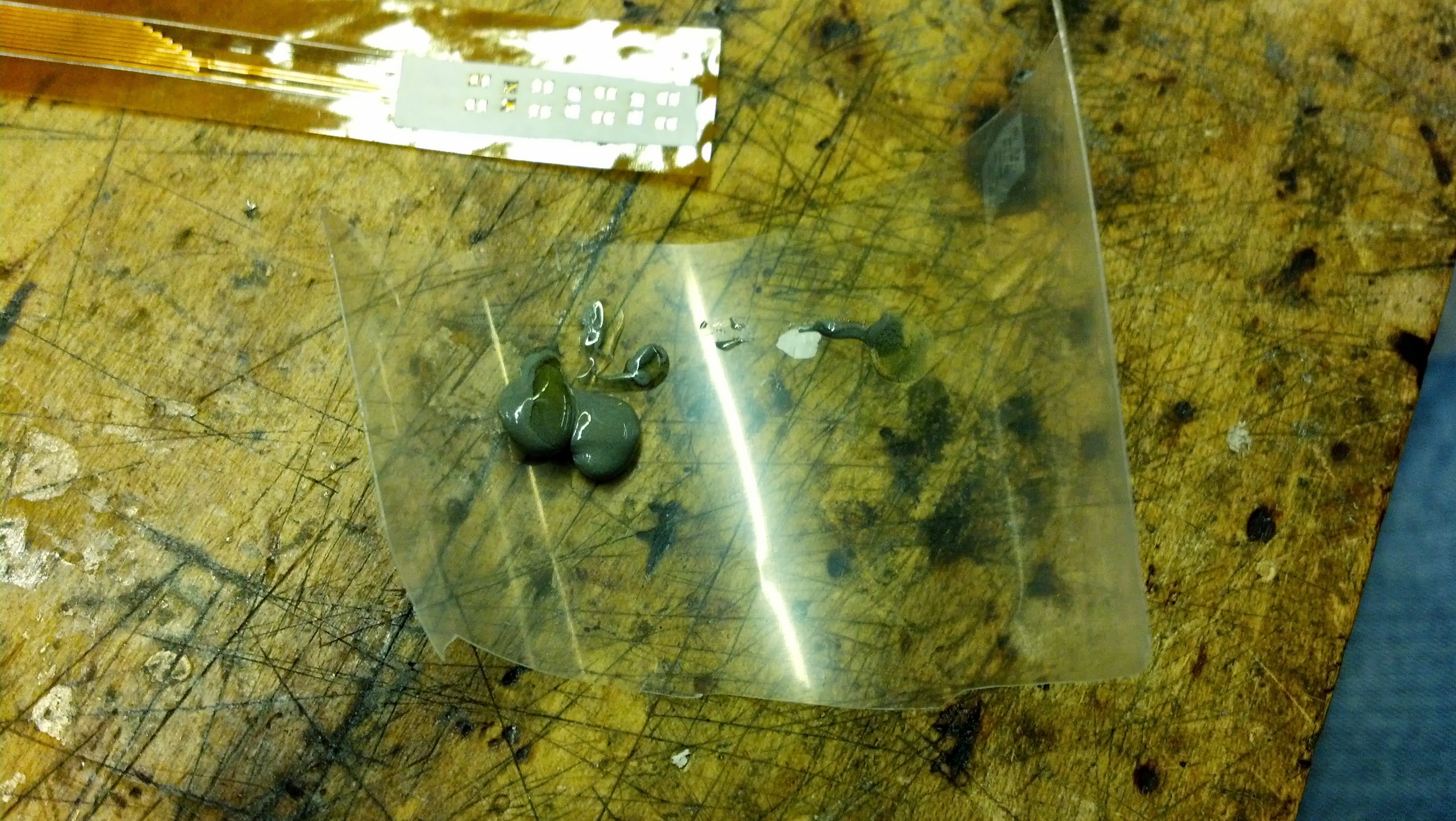
- Apply the solder paste.
- It dries out quickly so don�t leave the bottle open too long.
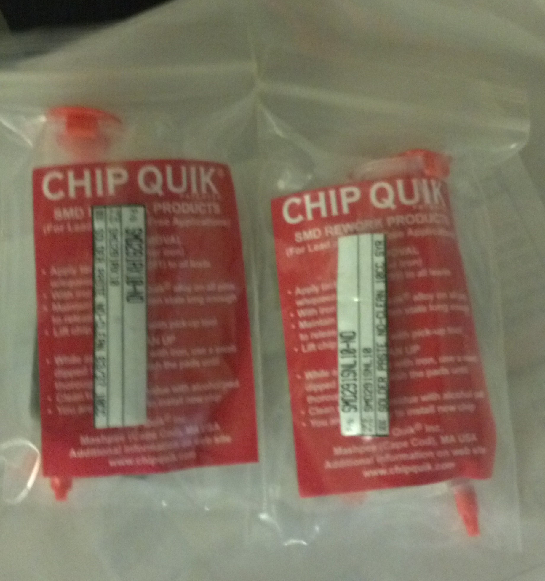
- The kind with lead (Pb) re-flows faster and is more convenient to work with, but it is more dangerous than the lead-free one. You can choose.
- Squirt about half a dime onto a disposable plastic surface, like a dixie cup. Look at it under the microscope, mix it if the small lead balls are not mixed in adequately.
- Put it on a small spatula and spread a thin layer over the mask. Make sure all the pads cavities are filled. Only go up to the top of the tape, no higher or else your board will short.
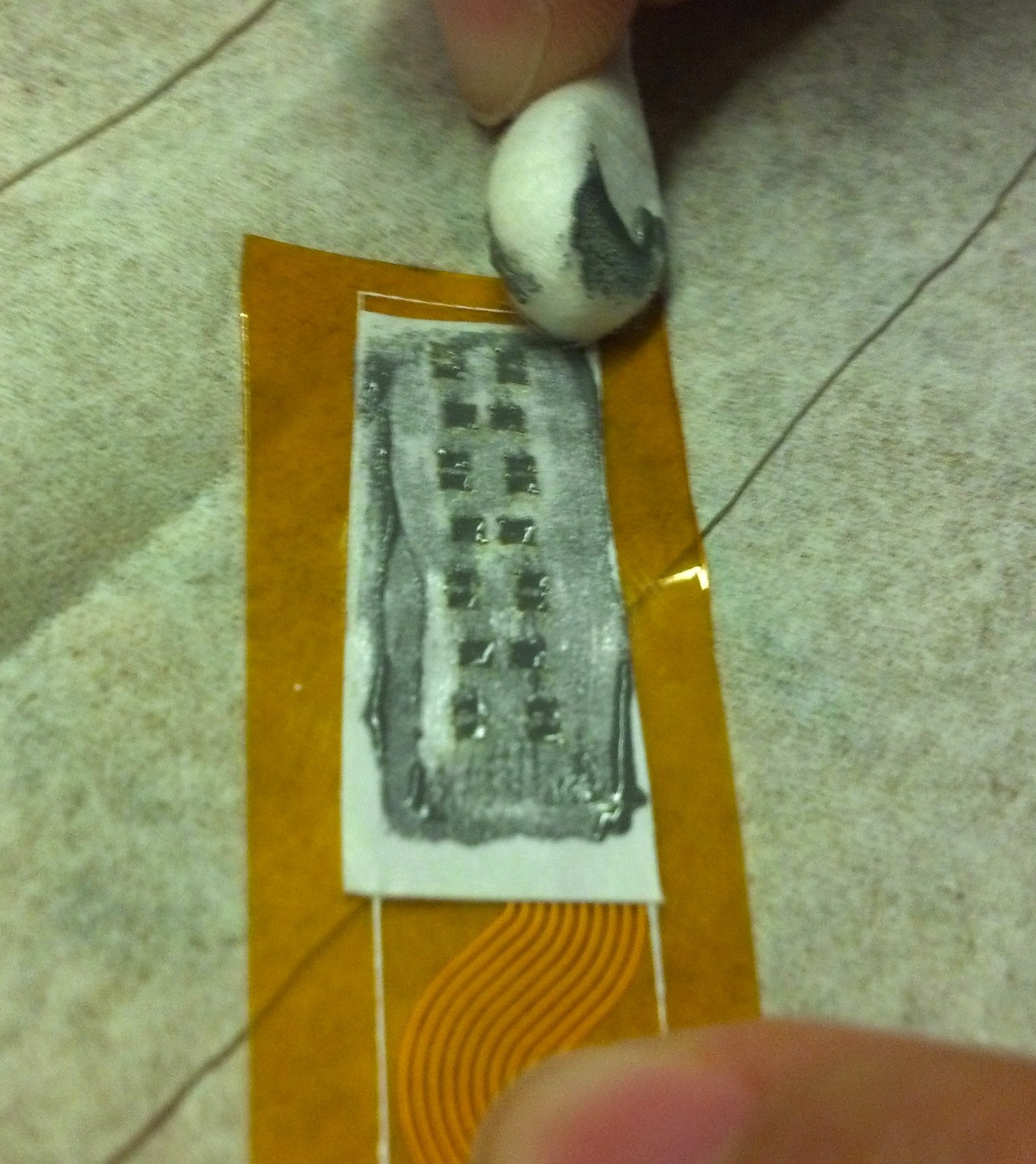
- Apply the solder paste.
- Remove the stencil and clean up any unwanted solder with a Q-tip. You can also add extra solder paste by hand if you need to with the tip of a tweezer or other sharp tip.
4) Place the components on the board.
- Use tweezers to pick and place the parts. This can be a little tricky. Try not to drink a ton of caffeine right before you start or else your hands might shake too much.
- Review the placement and orientation of your components under the microscope. You will hopefully be able to see if there are any shorts.
- If you have accidentally shorted leads and want to start again, use isopropyl to wipe off the solder paste from the PCB. Consider using new components on your second attempt.
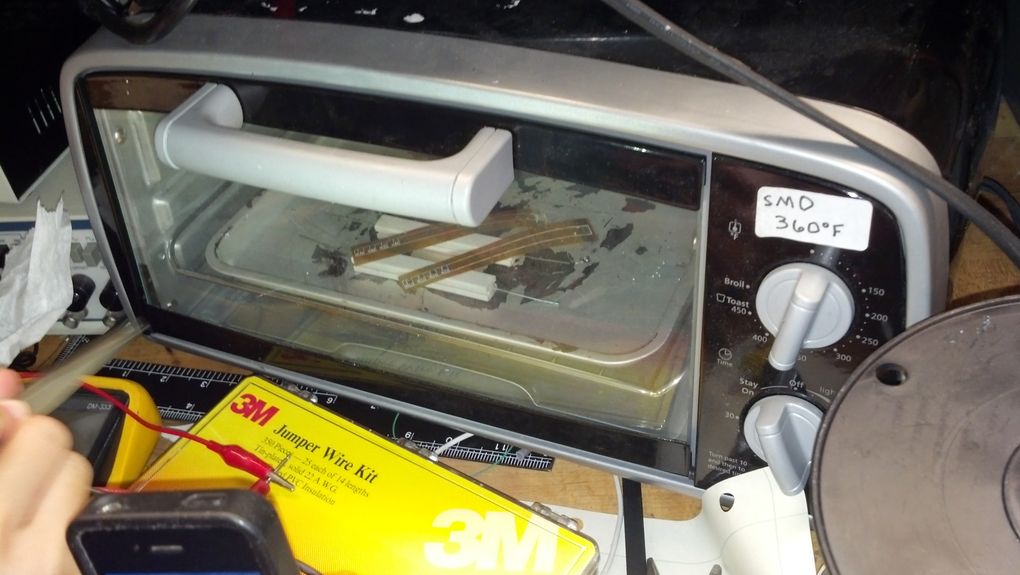
5) Heat the PCB to flow the solder:
- There are two heating methods to flow the solder-paste:
- Heat plate = even heat but can only do one-sided boards
- Toaster oven = IR heat, so be careful with IR sensors... check data sheet for IR tolerance. This is the option we usually use in lab, and will describe below.
- Preheat oven to 360 degrees. Wait until the heating elements turn red, then it is probably pre-heated or close enough. Place the board in the oven on top of the large ceramic resistors. Watch until the solder paste gets shiny (just 20-40 seconds); this tells you that the solder has flowed.
- There are two heating methods to flow the solder-paste:
6) Check the circuit and make fixes:
- Check for shorts under the microscope.
- Use a digital multimeter to check for shorts.
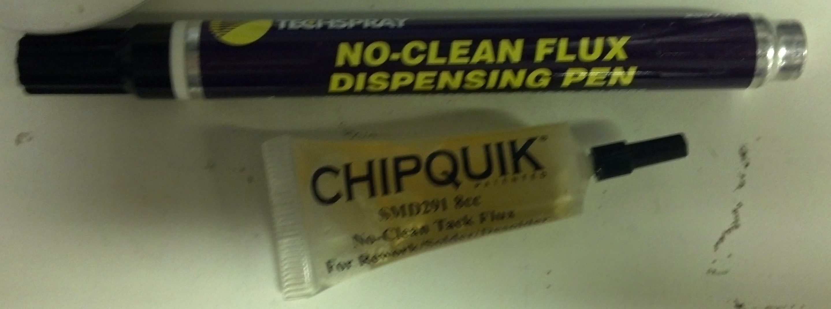
- There are a variety of creative ways to clean up a PCB that has gone wrong you may get creative:
- Remove components using heat gun at 360 degrees with a nozzle to redirect the heat on the area of interest. Grab onto the component with tweezers and when the solder flows, pull it off.
- Use flux.
7) Clean up the soldering station and your tools with soap and water.
Quick prototyping option: Print a circuit using conductive ink
The group who made it is AgIC: http://agic.cc/
This is a good double-check for simple circuits (single layer). You can use the silver inkjet printer in BDML to print onto PET plastic film or photo paper. The circuit resolution is pretty good and it is worth some experimenting. The resistance of traces will be higher than, for example, copper on kapton. AliceWu has some experience with designing and making circuits for this printer.
Interesting new Arduino-compatible paper-thin boards and components
https://www.kickstarter.com/projects/1030661323/printoo-paper-thin-flexible-arduinotm-compatible-m
From AliceWu 15 April 2014
From HannahStuart 30 June 2014
From CaitlinClancy 7 July 2014